
Market Report · July 29, 2026

Key data points: The growth forecast = 8.1% annually for the next 7 years. Scroll below to get more insights. This market report covers trends, opportunities and forecasts in semiconductor silicon wafer market to 2031 by type (300mm wafers, 200mm wafers, and small diameter wafers (100, 150mm)), application (memory, logic/MPU, analog, discrete device & sensor, and others), and region (North America, Europe, Asia Pacific, and the Rest of the World)
We'll send your sample report shortly.
• Lucintel forecasts that, within the type category, 300mm wafer is expected to witness higher growth over the forecast period.
• Within the application category, memory is expected to witness the highest growth.
• In terms of region, APAC is expected to witness the highest growth over the forecast period. Gain valuable insights for your business decisions with our comprehensive 150+ page report. Sample figures with some insights are shown below.
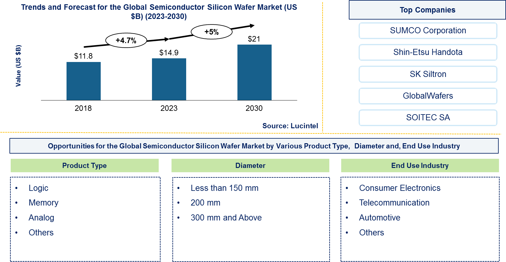
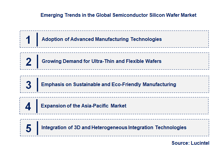
• Adoption of Advanced Manufacturing Technologies: The industry is increasingly integrating automation, AI, and machine learning into wafer fabrication processes. These technologies improve precision, reduce defects, and enhance yield rates, leading to higher efficiency and lower costs. Advanced manufacturing also enables the production of smaller, more powerful chips, meeting the demands of next-generation devices. This trend is transforming traditional production methods, making them more sustainable and scalable, and positioning companies to better respond to market fluctuations and technological innovations.
• Growing Demand for Ultra-Thin and Flexible Wafers: As consumer electronics and wearable devices become more sophisticated, there is a rising need for ultra-thin, flexible silicon wafers. These wafers enable the development of lightweight, bendable, and compact devices, expanding application possibilities in healthcare, automotive, and IoT sectors. The trend drives innovation in wafer materials and processing techniques, pushing manufacturers to develop new solutions that maintain performance while reducing thickness. This shift is opening new markets and creating opportunities for customized, high-performance wafers tailored to specific device requirements.
• Emphasis on Sustainable and Eco-Friendly Manufacturing: Environmental concerns are prompting the industry to adopt greener practices, such as reducing water and energy consumption, utilizing recycled materials, and minimizing hazardous waste. Companies are investing in sustainable wafer production processes to meet regulatory standards and consumer expectations for eco-conscious products. This trend not only reduces the environmental footprint but also enhances brand reputation and operational efficiency. As sustainability becomes a key differentiator, manufacturers are innovating to develop more eco-friendly materials and processes, shaping the future of responsible semiconductor manufacturing.
• Expansion of the Asia-Pacific Market: The Asia-Pacific region continues to dominate the silicon wafer industry due to its large manufacturing base, technological expertise, and growing consumer electronics market. Countries like China, South Korea, and Taiwan are investing heavily in expanding production capacities and technological capabilities. This regional growth is driven by rising demand for semiconductors in smartphones, PCs, and automotive electronics. The expansion enhances supply chain resilience and reduces dependency on Western markets, while also fostering regional innovation hubs. This trend is solidifying Asia-Pacific’s position as the global leader in silicon wafer manufacturing.
• Integration of 3D and Heterogeneous Integration Technologies: The push toward 3D stacking and heterogeneous integration is revolutionizing wafer design and functionality. These technologies enable stacking multiple chips vertically, increasing performance and reducing footprint. They facilitate the integration of different materials and functionalities on a single wafer, supporting the development of more complex, high-performance devices such as AI chips and advanced sensors. This trend is driving innovation in wafer architecture, demanding new manufacturing techniques and materials. It is fundamentally transforming the capabilities of silicon wafers, opening avenues for next-generation electronic devices with unprecedented performance. In summary, these emerging trends are collectively reshaping the semiconductor silicon wafer market by fostering innovation, enhancing sustainability, and expanding regional influence. They are enabling the industry to meet the evolving demands of high-performance electronics while addressing environmental and supply chain challenges. As these trends continue to develop, they will drive the market toward greater efficiency, customization, and technological sophistication, ensuring its growth and relevance in the rapidly advancing electronics landscape.
• Technological Innovations: Adoption of advanced manufacturing techniques such as chemical mechanical planarization (CMP) and ion implantation has improved wafer quality, enabling higher performance and reliability in electronic devices. This development enhances product efficiency and reduces defect rates, positively impacting the market by meeting the increasing demand for miniaturized and high-performance chips.
• Expansion of Capacity: Major players are investing in expanding production capacities to meet rising global demand. New fabrication plants and upgraded facilities are boosting supply, reducing lead times, and addressing shortages. This development stabilizes the supply chain, supports market growth, and helps meet the escalating needs of consumer electronics, automotive, and industrial sectors.
• Focus on Sustainability: Companies are adopting eco-friendly manufacturing processes, including water recycling and reduction of hazardous chemicals. These initiatives aim to minimize environmental impact and comply with stricter regulations. The shift towards sustainable practices enhances corporate responsibility, appeals to environmentally conscious consumers, and positions companies favorably in the market.
• Geographical Diversification: Market players are expanding operations into emerging regions such as Southeast Asia and India to diversify supply chains and reduce dependency on traditional manufacturing hubs. This geographical diversification mitigates risks associated with geopolitical tensions and supply disruptions, ensuring a more resilient market environment.
• Integration of AI and Automation: The incorporation of artificial intelligence and automation in wafer fabrication processes has increased precision, reduced errors, and improved efficiency. This technological integration accelerates production cycles, lowers costs, and enhances quality control, thereby strengthening competitive advantage and supporting market expansion. In summary, these recent developments are collectively driving growth, improving supply chain resilience, and promoting sustainable practices within the semiconductor silicon wafer market. They are enabling manufacturers to meet rising global demand, innovate continuously, and adapt to evolving regulatory and environmental standards, ultimately shaping a more robust and sustainable industry landscape.
• Consumer Electronics: Expanding demand for smartphones, tablets, and wearable devices is driving silicon wafer needs. As consumer electronics become more sophisticated, the demand for high-performance, miniaturized wafers increases, boosting market growth and encouraging innovation in wafer manufacturing processes.
• Automotive Industry: The rise of electric vehicles and autonomous driving systems is fueling the need for advanced silicon wafers. These wafers are critical for sensors, power modules, and integrated circuits, enabling smarter, more efficient vehicles and opening new revenue streams for manufacturers.
• Industrial Applications: Automation, robotics, and IoT integration in manufacturing are increasing the demand for durable, high-quality silicon wafers. These applications require wafers with enhanced performance and reliability, fostering innovation and expanding market reach.
• Telecommunications: The rollout of 5G networks necessitates advanced semiconductor components, including silicon wafers. The demand for high-frequency, high-speed chips is propelling growth in this segment, supporting faster connectivity and new service offerings.
• Healthcare: The growing adoption of medical devices, imaging systems, and wearable health monitors relies on high-performance silicon wafers. This application segment is expanding as healthcare providers seek more precise, reliable, and miniaturized electronic solutions. In summary, these key growth opportunities across applications are significantly impacting the semiconductor silicon wafer market by driving innovation, increasing demand, and fostering competitive differentiation. As industries evolve, the market is poised for sustained expansion, with companies investing in advanced technologies to meet emerging needs and capitalize on new revenue streams.
• Technological Innovation: The continuous development of advanced manufacturing processes, such as ultra-thin wafers and improved doping techniques, enhances wafer performance and quality. This innovation enables the production of smaller, faster, and more energy-efficient semiconductor devices, fueling demand. As consumer electronics, automotive, and industrial sectors evolve, the need for high-quality silicon wafers increases, making technological progress a key growth driver.
• Growing Electronics Industry: The surge in consumer electronics, including smartphones, tablets, and wearables, significantly boosts demand for silicon wafers. The expansion of the Internet of Things (IoT) and smart devices further amplifies this trend. As these devices require sophisticated semiconductors, the electronics industry’s growth directly correlates with increased wafer consumption, supporting market expansion.
• Investment in Semiconductor Manufacturing: Governments and private entities worldwide are investing heavily in semiconductor fabrication facilities to meet rising demand. Initiatives like the CHIPS Act in the U.S. aim to boost domestic production. These investments lead to increased capacity and technological capabilities, reducing supply shortages and fostering market growth.
• Environmental and Sustainability Regulations: Stricter environmental standards influence manufacturing processes, pushing companies to adopt eco-friendly practices. This includes reducing hazardous waste and energy consumption during wafer production. While compliance may increase costs initially, it encourages innovation and sustainable growth, shaping the market’s future trajectory. The challenges facing semiconductor silicon wafer market include:-
• Supply Chain Disruptions: The global semiconductor supply chain faces disruptions due to geopolitical tensions, pandemics, and logistical issues. These disruptions cause delays in wafer production and shortages, impacting downstream industries. Overcoming these challenges requires diversification of supply sources and strategic stockpiling, which can increase operational costs.
• High Capital Expenditure: Establishing advanced wafer fabrication facilities demands significant investment in equipment, technology, and skilled labor. This high capital requirement limits entry for new players and constrains expansion for existing manufacturers. Economic uncertainties can further hinder funding, affecting market competitiveness and innovation pace.
• Technological Complexity and R&D Costs: Developing next-generation wafers involves complex processes and substantial research and development expenses. Keeping pace with rapid technological changes necessitates continuous innovation, which can be costly and risky. Failure to innovate effectively may result in loss of market share and reduced profitability. In summary, the semiconductor silicon wafer market is driven by technological advancements, increasing electronics demand, strategic investments, and sustainability initiatives. However, it faces challenges such as supply chain vulnerabilities, high capital costs, and technological complexities. These factors collectively influence market dynamics, requiring stakeholders to adapt strategically. While growth prospects remain promising, addressing these challenges is crucial for sustained development and competitiveness in the evolving semiconductor landscape.
• Shin-Etsu Chemical
• SUMCO
• GlobalWafers
• Siltronic
• SK Siltron
• FST Corporation
• Wafer Works Corporation
• National Silicon Industry Group
• Zhonghuan Advanced Semiconductor Materials
• Zhejiang Jinruihong Technologies
• 300mm Wafers
• 200mm Wafers
• Small Diameter Wafers (100, 150mm)
• Memory
• Logic/MPU
• Analog
• Discrete Device & Sensor
• Others
• North America
• Europe
• Asia Pacific
• The Rest of the World
• United States: The US market is witnessing significant investments in advanced manufacturing technologies and R&D, with a focus on high-purity silicon wafers for cutting-edge applications like AI and 5G. Major companies are expanding capacity and forming strategic alliances to maintain technological leadership. Government initiatives such as the CHIPS Act aim to boost domestic production and reduce reliance on imports, fostering innovation and supply chain resilience. The US also emphasizes sustainable manufacturing practices, including recycling and energy-efficient processes, to meet environmental standards and reduce costs.
• China: China is rapidly expanding its semiconductor manufacturing capabilities, with substantial government support through policies like the "Made in China 2025" plan. The country is investing heavily in domestic silicon wafer production to reduce dependency on foreign suppliers. Chinese firms are adopting advanced fabrication techniques and increasing capacity to serve the growing demand for consumer electronics and automotive chips. Efforts are also underway to develop high-performance, large-diameter wafers, aiming to become a global leader in semiconductor manufacturing and supply chain independence.
• Germany: Germany’s market is characterized by a focus on high-precision, high-quality silicon wafers for automotive, industrial, and medical applications. The country is leveraging its strong engineering expertise and technological innovation to develop specialized wafers with enhanced performance. German companies are investing in sustainable production methods and digitalization to improve efficiency and reduce environmental impact. Collaborations with research institutions are fostering advancements in wafer technology, positioning Germany as a key player in the European semiconductor ecosystem.
• India: India is emerging as a significant player in the semiconductor supply chain, with government initiatives promoting local manufacturing and R&D. The country is investing in establishing semiconductor fabrication units and silicon wafer production facilities to support domestic demand and export ambitions. Focus areas include developing cost-effective, high-quality wafers for consumer electronics and automotive sectors. India is also fostering partnerships with global firms to acquire advanced technology and build a robust ecosystem for semiconductor manufacturing, aiming to become a regional hub.
• Japan: Japan continues to be a leader in high-quality silicon wafer production, emphasizing innovation in materials and process technology. The country is investing in next-generation wafer technologies, including ultra-thin and large-diameter wafers, to meet the demands of advanced electronics and automotive industries. Japanese firms are also focusing on sustainable manufacturing practices and supply chain resilience amid global geopolitical tensions. Collaborations with international partners and government support are driving technological advancements, ensuring Japan maintains its competitive edge in the global semiconductor silicon wafer market.

• Shin-Etsu Chemical
• SUMCO
• GlobalWafers
• Siltronic
• SK Siltron
• FST Corporation
• Wafer Works Corporation
• National Silicon Industry Group
• Zhonghuan Advanced Semiconductor Materials
• Zhejiang Jinruihong Technologies Q5. Which semiconductor silicon wafer market segment will be the largest in future? Answer: Lucintel forecasts that, within the type category, 300mm wafer is expected to witness higher growth over the forecast period. Q6. In semiconductor silicon wafer market, which region is expected to be the largest in next 5 years? Answer: In terms of region, APAC is expected to witness the highest growth over the forecast period. Q7. Do we receive customization in this report? Answer: Yes, Lucintel provides 10% customization without any additional cost.


Choose a license that fits your team. Instant PDF delivery.
Prices exclude taxes. Instant delivery. Custom licensing available on request.
Market Report · July 29, 2026
Market Report · July 20, 2026
Market Report · July 20, 2026
Trusted partner for strategic intelligence and business growth


Receive a complimentary market analysis tailored to your industry. Our analysts will identify key growth opportunities and competitive dynamics specific to your business.

Market size, growth rate, and key trend analysis for your specific sector.

Top competitor positioning and market share analysis.

Strategic recommendations backed by data-driven insights.
Get curated market intelligence and competitive moves straight to your inbox.
By subscribing, you agree to receive our monthly insights. Unsubscribe anytime.
Receive a complimentary market analysis tailored to your industry. Our analysts will identify key growth opportunities and competitive dynamics specific to your business.
Market size, growth rate, and key trend analysis for your specific sector.
Top competitor positioning and market share analysis.
Strategic recommendations backed by data-driven insights.
Get curated market intelligence, emerging trends, and competitive moves straight to your inbox each month.
By subscribing, you agree to receive our monthly insights. Unsubscribe anytime.
We'll send your sample report shortly.