
Market Report · July 22, 2026

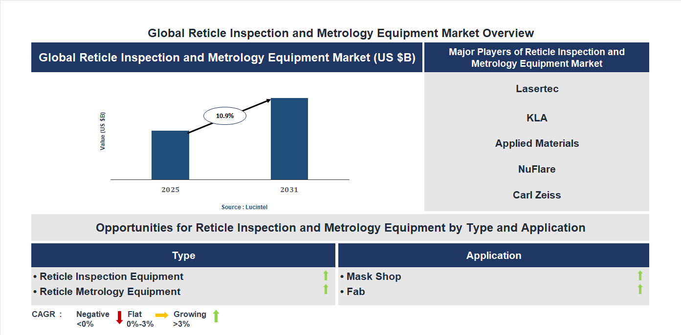
Key data points: The growth forecast = 10.9% annually for the next 7 years. Scroll below to get more insights. This market report covers trends, opportunities and forecasts in reticle inspection and metrology equipment market to 2031 by type (reticle inspection equipment and reticle metrology equipment), application (mask shop and fab), and region (North America, Europe, Asia Pacific, and the Rest of the World)
We'll send your sample report shortly.
• Lucintel forecasts that, within the type category, reticle inspection equipment is expected to witness higher growth over the forecast period.
• Within the application category, fab is expected to witness higher growth.
• In terms of region, APAC is expected to witness the highest growth over the forecast period. Gain valuable insights for your business decisions with our comprehensive 150+ page report. Sample figures with some insights are shown below.
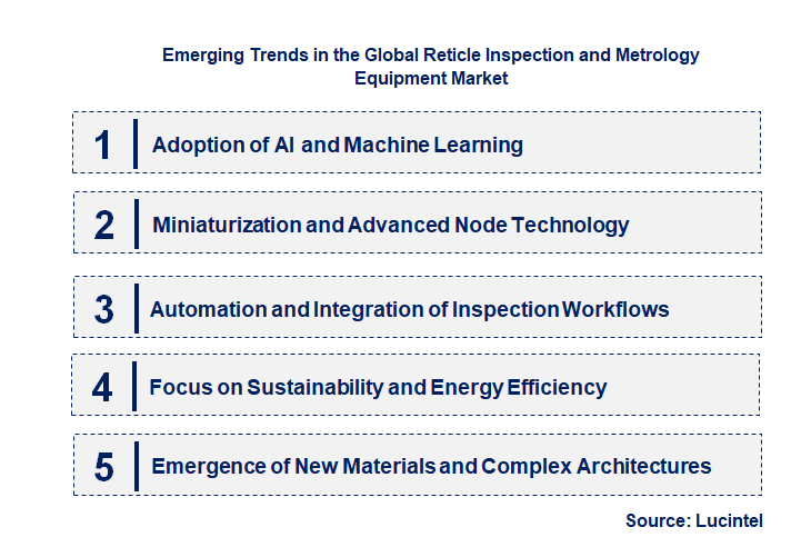
• Adoption of AI and machine learning: Integration of AI and machine learning algorithms is revolutionizing reticle inspection and metrology processes by enabling real-time defect detection and predictive maintenance. These technologies improve accuracy, reduce false positives, and speed up analysis, leading to higher throughput and lower costs. Companies like ASML and Nikon are investing heavily in AI-driven solutions to stay competitive. This trend enhances overall quality control, minimizes downtime, and supports the production of increasingly complex semiconductor devices, making manufacturing more efficient and reliable.
• Miniaturization and advanced node technology: The push towards smaller process nodes, such as 3nm and below, demands higher precision in inspection and measurement. Equipment must detect minute defects at nanometer scales, which drives innovation in optical and electron-beam technologies. This trend is critical for companies like lam research and Tokyo electron, as it ensures the integrity of tiny features on chips. The impact is a significant increase in the complexity of inspection tools, enabling manufacturers to meet the stringent quality standards required for next-generation semiconductors.
• Automation and integration of inspection workflows: Increasing automation in reticle inspection and metrology is streamlining manufacturing processes. Automated defect classification, data management, and integration with fabrication equipment reduce manual intervention, minimize errors, and accelerate production cycles. Companies such as KLA Corporation are developing comprehensive platforms that combine multiple inspection steps into seamless workflows. This trend enhances operational efficiency, reduces time-to-market, and supports high-volume manufacturing, which is essential for meeting global demand for advanced electronic devices.
• Focus on sustainability and energy efficiency: Environmental concerns and energy costs are prompting the industry to develop more sustainable inspection and metrology solutions. Innovations include energy-efficient light sources, reduced waste generation, and equipment designed for lower power consumption. Companies like Nikon are incorporating eco-friendly features into their systems. This trend not only reduces the environmental footprint but also lowers operational costs for manufacturers, aligning with global sustainability goals and regulatory requirements, and ensuring long-term viability of production facilities.
• Emergence of new materials and complex architectures: As new materials like silicon carbide and gallium nitride are adopted for specialized applications, inspection equipment must adapt to handle these materials unique properties. Additionally, the rise of 3D architectures and heterogeneous integration complicates defect detection and measurement. Companies such as ASML are developing specialized tools to address these challenges. This trend expands the market scope, requiring innovative solutions to ensure quality in emerging semiconductor technologies, and supports the development of more advanced, high-performance electronic devices. In summary, these trends are fundamentally transforming the reticle inspection and metrology equipment market by enhancing precision, efficiency, and sustainability. They enable semiconductor manufacturers to meet the demands of next-generation devices, ensuring higher quality and faster production cycles. As a result, the market is becoming more innovative, competitive, and aligned with the evolving needs of the global electronics industry.
• Technological integration of AI and machine learning: Companies like asml and kLA are incorporating AI algorithms into inspection tools, significantly improving defect detection accuracy and processing speed. This advancement reduces false positives and enhances overall efficiency, leading to higher yields and lower costs for semiconductor manufacturers.
• Miniaturization and higher resolution capabilities: firms such as nanometrics and hitachi are developing next-generation equipment with ultra-high resolution and smaller form factors. These innovations enable more precise inspection of increasingly complex and smaller reticles, supporting the trend toward smaller chip geometries and advanced nodes.
• Expansion of automation and smart systems: companies like asml and kLA are deploying automated inspection systems integrated with real-time data analytics. This automation reduces manual intervention, accelerates inspection cycles, and improves consistency, thereby increasing throughput and reducing operational costs.
• Growing adoption in emerging markets: players such as nanometrics and hitachi are expanding their presence in Asia-Pacific and other emerging regions. This expansion is driven by rising semiconductor manufacturing activities and government initiatives, broadening the market base and increasing demand for inspection and metrology solutions.
• Development of environmentally sustainable equipment: firms like asml and kLA are focusing on eco-friendly innovations, including energy-efficient systems and reduced chemical usage. These efforts align with global sustainability goals and appeal to environmentally conscious clients, fostering market growth. In summary, these key developments are transforming the reticle inspection and metrology equipment market by enhancing technological capabilities, increasing efficiency, and expanding global reach. The integration of AI, miniaturization, automation, regional expansion, and sustainability initiatives are collectively driving growth, improving product offerings, and enabling manufacturers to meet the evolving demands of the semiconductor industry.
• Miniaturization of Semiconductor Devices: As device sizes shrink, the need for ultra-precise inspection and metrology tools increases, driving demand for high-resolution equipment that can detect minute defects, thereby improving yield and reliability.
• Advanced EUV Lithography Inspection: The adoption of extreme ultraviolet (EUV) lithography necessitates specialized inspection tools to ensure pattern fidelity, creating opportunities for companies to develop tailored solutions that enhance process control.
• 3D Packaging and System-in-Package (SiP) Inspection: The rise of 3D integrated circuits and SiP technologies requires sophisticated inspection systems capable of analyzing complex multilayer structures, expanding the market for multi-dimensional metrology solutions.
• AI-Driven Inspection and Data Analytics: Incorporating artificial intelligence and machine learning into inspection processes enables faster defect detection and predictive maintenance, significantly improving efficiency and reducing downtime.
• Expansion into Emerging Markets: Growing semiconductor manufacturing activities in regions like Asia-Pacific open new avenues for localized inspection and metrology solutions, fostering market growth through regional customization and support. These growth opportunities are collectively transforming the reticle inspection and metrology equipment market by enhancing technological capabilities, improving process efficiencies, and expanding geographical reach. As a result, the market is poised for sustained growth, driven by innovation and increasing demand for precision in semiconductor manufacturing.
• technological innovation: The rapid pace of technological innovation in semiconductor manufacturing necessitates advanced inspection and metrology tools. As device geometries shrink, the need for precise, high-resolution equipment becomes critical to ensure quality and yield. Companies like ASML and Nikon are investing heavily in R&D to develop next-generation systems capable of handling smaller nodes, which directly fuels market growth. This ongoing innovation not only improves accuracy but also reduces inspection time, enabling manufacturers to meet tight production schedules and quality standards efficiently.
• increasing demand for smaller, more complex chips: The surge in demand for advanced electronics, IoT devices, and 5G infrastructure has led to the production of highly complex chips with intricate designs. Reticle inspection and metrology equipment are essential for verifying these designs at every stage of manufacturing. As complexity increases, so does the need for sophisticated tools capable of detecting minute defects and ensuring pattern fidelity. This trend drives market expansion as semiconductor manufacturers seek reliable solutions to maintain high yields and performance standards.
• regulatory and quality standards: Stringent industry regulations and quality standards, such as ISO certifications and SEMI standards, compel manufacturers to adopt high-precision inspection and metrology tools. These standards ensure product reliability and safety, especially in critical applications like automotive and aerospace. Compliance requires investment in advanced equipment capable of detailed defect analysis and process control. This regulatory environment encourages market growth by pushing companies to upgrade their inspection capabilities to meet evolving compliance requirements.
• technological integration and automation: The integration of AI, machine learning, and automation into inspection and metrology systems enhances accuracy, speed, and data analysis capabilities. Automated defect detection reduces human error and increases throughput, which is vital for high-volume semiconductor production. Companies like kLA and hitachi are developing intelligent systems that streamline inspection processes, reduce costs, and improve yield rates. This technological integration is a key driver, enabling manufacturers to achieve higher efficiency and better process control in a competitive market. The challenges in the reticle inspection and metrology equipment market are:
• high equipment costs: The advanced nature of reticle inspection and metrology tools results in significant capital expenditure for semiconductor manufacturers. The high costs can be prohibitive, especially for smaller players or those in emerging markets, limiting widespread adoption. Additionally, ongoing maintenance and calibration expenses add to the financial burden. This financial barrier can slow market growth and restrict access to cutting-edge technology, impacting overall industry innovation and competitiveness.
• technological complexity and skill gap: The sophisticated nature of these systems requires specialized knowledge for operation and maintenance. The skill gap among technicians and engineers can hinder effective utilization, leading to underperformance or errors. Training personnel and ensuring consistent system performance pose ongoing challenges for manufacturers, especially in regions with limited technical expertise. Overcoming this complexity is essential for maximizing the benefits of advanced inspection and metrology equipment.
• rapid technological obsolescence: The fast-paced evolution of semiconductor technology results in equipment becoming obsolete quickly. Companies face pressure to continually upgrade or replace systems to stay competitive, which incurs substantial costs. This rapid obsolescence can lead to increased capital expenditure and operational disruptions, complicating long-term planning. Managing technological lifecycle and ensuring compatibility with new manufacturing processes remain significant hurdles for industry stakeholders. In summary, the reticle inspection and metrology equipment market is shaped by technological advancements, increasing chip complexity, and regulatory demands, which collectively drive growth. However, high costs, technological complexity, and rapid obsolescence present notable challenges. These factors influence market dynamics, requiring companies to innovate continuously and strategize effectively. Overall, the markets future depends on balancing these drivers and challenges to foster sustainable growth and technological progress.
• Lasertec
• KLA
• Applied Materials
• NuFlare
• Carl Zeiss
• Advantest
• MueTec
• Suzhou Vptek
• Hefei Yuwei Semiconductor Technology
• Horiba
• Reticle Inspection Equipment
• Reticle Metrology Equipment
• Mask Shop
• Fab
• North America
• Europe
• Asia Pacific
• The Rest of the World
• United States: The US market sees significant innovation with companies like KLA and lam research investing heavily in AI-driven inspection systems. There is a focus on automation and integration of machine learning to improve defect detection accuracy. The US government is also supporting R&D initiatives to maintain technological leadership, with increased collaborations between industry and academia. The adoption of advanced metrology tools is accelerating in semiconductor fabs, driven by demand for smaller nodes and higher yields.
• China: China is rapidly expanding its reticle inspection capabilities through government-backed initiatives and local companies such as naura and accretech. The focus is on reducing reliance on foreign technology by developing indigenous solutions. Investments are directed toward high-throughput inspection systems and automation to support domestic semiconductor manufacturing. Strategic partnerships with international firms are also fostering technology transfer and skill development, aiming to boost self-sufficiency in advanced inspection equipment.
• Germany: Germany remains a key player in high-precision metrology, with companies like zeiss and essilor leading innovations in optical inspection systems. The emphasis is on enhancing measurement accuracy for advanced semiconductor nodes and integrating AI for predictive maintenance. The German market benefits from strong industrial automation and a focus on quality control, with collaborations between research institutes and industry driving technological advancements. Sustainability and energy efficiency are also prioritized in new equipment designs.
• India: India is witnessing a growing demand for reticle inspection and metrology tools driven by expanding semiconductor manufacturing and R&D activities. Companies like scantech and local startups are developing cost-effective solutions tailored for emerging markets. The government’s "Make in India" initiative encourages domestic production and technology development. Investments are focused on building local capabilities, with an emphasis on training skilled workforce and establishing testing facilities to support the growing semiconductor ecosystem.
• Japan: Japan continues to innovate in high-precision metrology, with companies such as tokyo electron and Nikon advancing inspection systems for next-generation chips. The focus is on miniaturization, higher throughput, and integration of AI for defect analysis. Japan’s strong semiconductor equipment manufacturing base is supported by government policies promoting technological leadership and international collaboration. The country is also investing in sustainable and energy-efficient inspection solutions to meet global environmental standards.
• Lasertec
• KLA
• Applied Materials
• NuFlare
• Carl Zeiss
• Advantest
• MueTec
• Suzhou Vptek
• Hefei Yuwei Semiconductor Technology
• Horiba Q5. Which reticle inspection and metrology equipment market segment will be the largest in future? Answer: Lucintel forecasts that, within the type category, reticle inspection equipment is expected to witness higher growth over the forecast period. Q6. In reticle inspection and metrology equipment market, which region is expected to be the largest in next 5 years? Answer: In terms of region, APAC is expected to witness the highest growth over the forecast period. Q7. Do we receive customization in this report? Answer: Yes, Lucintel provides 10% customization without any additional cost.


Choose a license that fits your team. Instant PDF delivery.
Prices exclude taxes. Instant delivery. Custom licensing available on request.
Market Report · July 22, 2026
Market Report · July 17, 2026
Market Report · July 17, 2026
Trusted partner for strategic intelligence and business growth


Receive a complimentary market analysis tailored to your industry. Our analysts will identify key growth opportunities and competitive dynamics specific to your business.

Market size, growth rate, and key trend analysis for your specific sector.

Top competitor positioning and market share analysis.

Strategic recommendations backed by data-driven insights.
Get curated market intelligence and competitive moves straight to your inbox.
By subscribing, you agree to receive our monthly insights. Unsubscribe anytime.
Receive a complimentary market analysis tailored to your industry. Our analysts will identify key growth opportunities and competitive dynamics specific to your business.
Market size, growth rate, and key trend analysis for your specific sector.
Top competitor positioning and market share analysis.
Strategic recommendations backed by data-driven insights.
Get curated market intelligence, emerging trends, and competitive moves straight to your inbox each month.
By subscribing, you agree to receive our monthly insights. Unsubscribe anytime.
We'll send your sample report shortly.