
Market Report · May 18, 2026

This market report covers trends, opportunities, and forecasts in the global cavity soi market to 2031 by technology (smart cut, bonding and layer transfer, high-temperature oxidation, buried oxide layer formation, and others), application (telecom, automotive, consumer electronics, medical, and others), and region (North America, Europe, Asia Pacific, and the Rest of the World)
We'll send your sample report shortly.
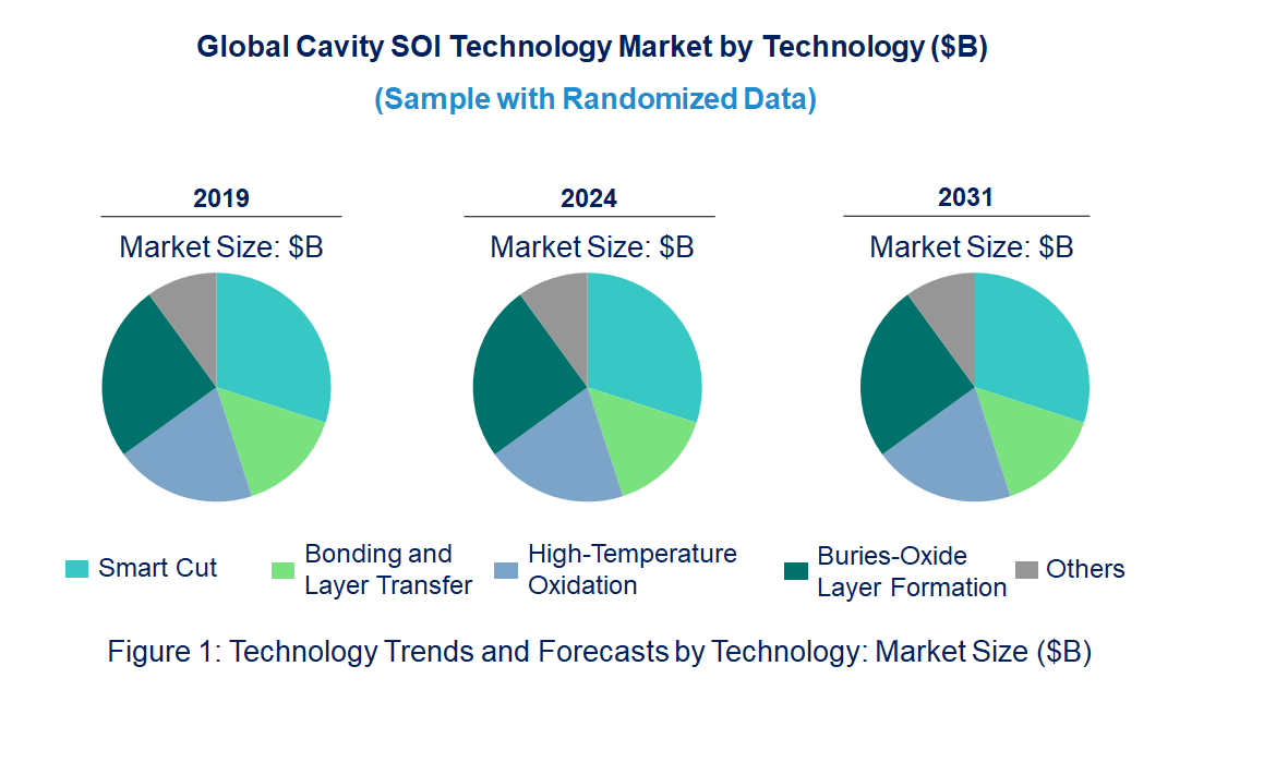
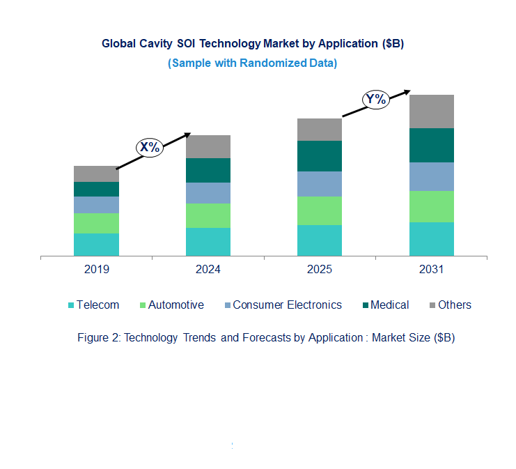
• Miniaturization of devices: As consumer electronics, automotive, and medical sectors demand smaller, more efficient devices, cavity SOI technology is evolving to support advanced packaging and miniaturization, especially in high-performance sensors and MEMS devices.
• Increased demand for 5G: The telecommunications industry is driving growth in the cavity SOI market, particularly for devices used in 5G infrastructure and applications. SOI wafers help deliver better speed, efficiency, and integration in 5G technology.
• Improved wafer yield and cost efficiency: Continuous developments in bonding and layer transfer technologies are enhancing wafer yield while reducing costs. This trend is essential to meet the demands of industries that require mass production at competitive prices.
• Advancements in MEMS devices: Cavity SOI technology is enabling more sophisticated and reliable MEMS (Micro-Electro-Mechanical Systems) sensors, contributing to the growth in industries like automotive (for sensors in autonomous vehicles) and healthcare (for wearable health devices).
• Focus on sustainability: As global industries push for sustainability, there’s an increasing shift towards environmentally friendly processes in SOI wafer production, reducing waste and energy consumption. In conclusion, these emerging trends in the cavity SOI market are reshaping the landscape, making it increasingly competitive, efficient, and aligned with the needs of high-demand industries such as telecommunications, automotive, and medical.
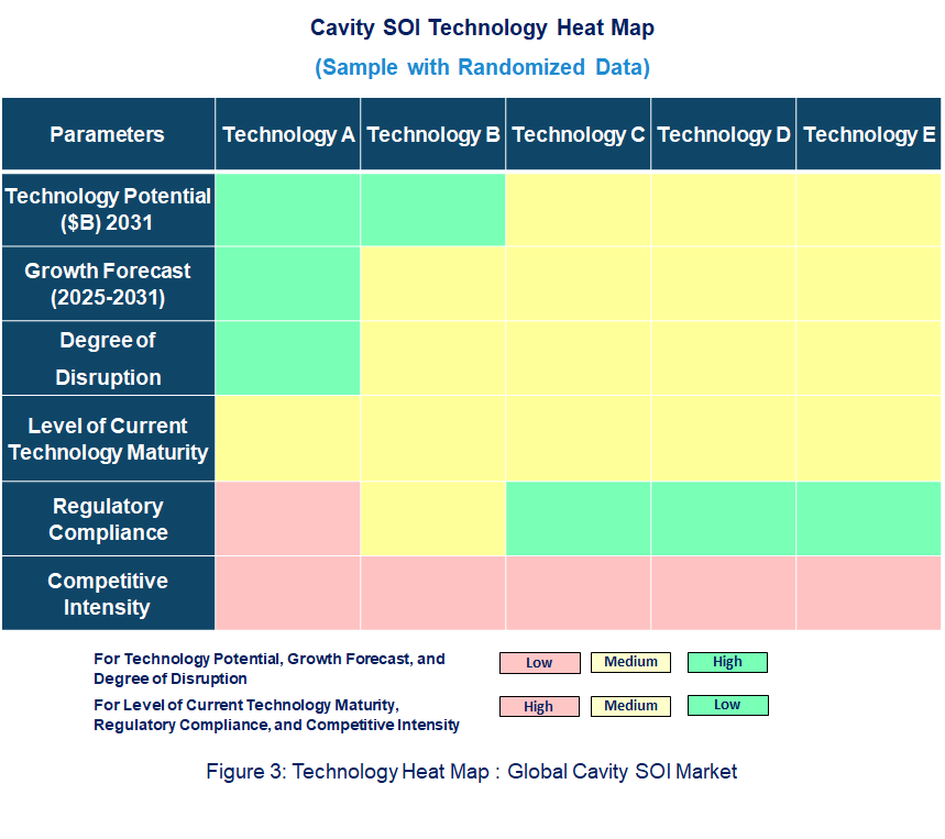
• Technology Potential: Cavity SOI technology enables the production of smaller, high-performance MEMS devices, which are critical for the ongoing trend of miniaturization across several industries, including mobile devices, wearables, and automotive sensors. The ability to isolate layers within a wafer allows for advanced sensor technologies that provide higher performance in terms of speed, power consumption, and reliability.
• Degree of Disruption: The disruption potential is substantial as Cavity SOI technology replaces traditional bulk silicon methods, enabling greater precision, smaller form factors, and lower power consumption. This is particularly impactful for the telecom and automotive sectors, where performance and miniaturization are key drivers.
• Current Technology Maturity Level: The core technologies used in Cavity SOI, such as smart cut, bonding and layer transfer, high-temperature oxidation, and buried oxide layer formation, have significant potential to enhance wafer performance by improving device miniaturization, efficiency, and integration.
• Regulatory Compliance: Regulatory standards, especially in automotive and medical industries, require compliance with safety, reliability, and environmental standards, pushing innovation in green and sustainable manufacturing processes. In conclusion, cavity SOI technology has significant disruptive potential and is mature enough to drive innovation in critical sectors, although addressing regulatory challenges and ensuring scalability remains essential for future growth.
• Soitec: Known for its advancements in smart cut technology, Soitec continues to lead in offering high-quality cavity SOI wafers for diverse applications, particularly in consumer electronics and automotive sectors. Soitec’s innovations in wafer bonding have enhanced the performance and miniaturization capabilities of electronic devices.
• Okmetic: Specializes in high-performance MEMS devices, and their cavity SOI wafers are critical in the development of sensors for automotive and industrial applications. Okmetic’s continuous improvement in wafer yields ensures reliable and cost-effective solutions for customers.
• Plutosemi: Known for its innovations in bonding and layer transfer technologies, Plutosemi has enabled the production of thinner and more reliable wafers, improving overall device performance, especially in telecommunications and medical applications.
• Microsemi: A major player in the development of high-temperature oxidation techniques, Microsemi provides high-quality wafers with better isolation and enhanced reliability, making them ideal for automotive, telecom, and industrial sectors.
• Globalwafers: Focuses on developing buried oxide layer formation technologies, which enhance wafer performance for MEMS applications. Globalwafers is also investing in sustainable manufacturing processes to meet the increasing demand for environmentally friendly solutions. In conclusion, these companies are playing a pivotal role in shaping the future of the cavity SOI market, driving technological advancements and innovations that meet the evolving needs of key industries.
• Increasing demand for high-performance semiconductors: The continuous need for more efficient semiconductors in telecom, automotive, and consumer electronics is a major driver for cavity SOI technology, fostering the adoption of advanced wafer technologies.
• Miniaturization trends: As electronic devices become smaller, the need for high-quality, compact semiconductors grows. Cavity SOI technology enables the development of smaller, more efficient MEMS devices, contributing to its market growth.
• Rising demand for 5G technology: The rapid expansion of 5G networks is driving demand for cavity SOI wafers, as these wafers help improve the speed, integration, and performance of 5G infrastructure.
• Advancements in MEMS devices: The development of advanced MEMS sensors for applications in automotive, medical, and consumer sectors is increasing demand for cavity SOI wafers, driving innovation and growth in the market. Challenges facing the global cavity SOI market are:
• High production costs: Despite advancements, the production of high-quality cavity SOI wafers is still costly, which can limit their adoption in cost-sensitive markets.
• Technological complexity: The complexity of production processes, especially with technologies like bonding and layer transfer, poses challenges for scaling production and achieving consistency.
• Environmental regulations: Increasing regulatory pressure for environmentally friendly manufacturing processes and sustainability can pose challenges for cavity SOI producers, requiring significant investments in green technologies. In conclusion, while the drivers create substantial growth opportunities for the cavity SOI market, the challenges highlight areas for innovation and improvement. Overcoming these challenges will be essential for the market to fully capitalize on its growth potential.
• Soitec
• Okmetic
• Plutosemi
• Microsemi
• Globalwafers
• Technology Readiness by Technology Type: Smart cut, bonding and layer transfer, high-temperature oxidation, and buried oxide layer formation are at different stages of technology readiness. Smart cut and bonding, and layer transfer are highly mature, widely adopted for commercial production of SOI wafers, and are well-established in the telecom and consumer electronics sectors. High-temperature oxidation is also mature, ensuring high-quality dielectric layers for advanced semiconductor devices. Buried oxide layer formation is crucial for niche applications in MEMS and high-performance sensors, and its technology is advancing rapidly, but may still be less widely applied. These technologies are highly competitive, with constant innovation driving improvements in performance, cost-efficiency, and scalability. Regulatory compliance remains a key consideration, especially in sectors like medical devices and automotive, where safety and environmental standards must be strictly met.
• Competitive Intensity and Regulatory Compliance: The competitive intensity in the cavity SOI market is high, with players vying for dominance through innovations in smart cut, bonding, and layer transfer, high-temperature oxidation, and buried oxide layer formation. Smart cut and bonding, and layer transfer dominate in terms of manufacturing scale and cost-effectiveness, while high-temperature oxidation and buried oxide layer formation focus on improving device performance. Regulatory compliance is a significant factor in the adoption of these technologies, particularly in industries like automotive and medical, where stringent standards exist. Compliance with environmental regulations, safety standards, and product reliability is crucial for these technologies to gain broader adoption.
• Disruption Potential of Different Technologies: In the cavity SOI market, technologies such as smart cut, bonding and layer transfer, high-temperature oxidation, and buried oxide layer formation offer different levels of disruption. Smart cut technology enables precise wafer thinning, contributing to greater miniaturization and better performance for applications like MEMS sensors. Bonding and layer transfer enable highly scalable and cost-effective manufacturing of stacked wafers, accelerating the development of complex devices. High-temperature oxidation is essential for creating high-quality insulator layers, improving the overall performance of semiconductors. Buried oxide layer formation ensures efficient isolation between layers, critical for reducing parasitic effects in high-speed applications. These technologies collectively foster the trend of miniaturization, improved energy efficiency, and cost reduction in semiconductor manufacturing, disrupting traditional bulk silicon approaches and enabling new applications in automotive, telecom, and consumer electronics.
• Smart Cut
• Bonding and Layer Transfer
• High-Temperature Oxidation
• Buried Oxide Layer Formation
• Others
• Telecom
• Automotive
• Consumer Electronics
• Medical
• Others
• North America
• Europe
• Asia Pacific
• The Rest of the World
• Latest Developments and Innovations in the Cavity SOI Technologies
• Companies / Ecosystems
• Strategic Opportunities by Technology Type


Choose a license that fits your team. Instant PDF delivery.
Prices exclude taxes. Instant delivery. Custom licensing available on request.
Market Report · May 18, 2026
Market Report · May 18, 2026
Market Report · May 18, 2026
Trusted partner for strategic intelligence and business growth


Receive a complimentary market analysis tailored to your industry. Our analysts will identify key growth opportunities and competitive dynamics specific to your business.

Market size, growth rate, and key trend analysis for your specific sector.

Top competitor positioning and market share analysis.

Strategic recommendations backed by data-driven insights.
Get curated market intelligence and competitive moves straight to your inbox.
By subscribing, you agree to receive our monthly insights. Unsubscribe anytime.
Receive a complimentary market analysis tailored to your industry. Our analysts will identify key growth opportunities and competitive dynamics specific to your business.
Market size, growth rate, and key trend analysis for your specific sector.
Top competitor positioning and market share analysis.
Strategic recommendations backed by data-driven insights.
Get curated market intelligence, emerging trends, and competitive moves straight to your inbox each month.
By subscribing, you agree to receive our monthly insights. Unsubscribe anytime.
We'll send your sample report shortly.