
Market Report · July 29, 2026

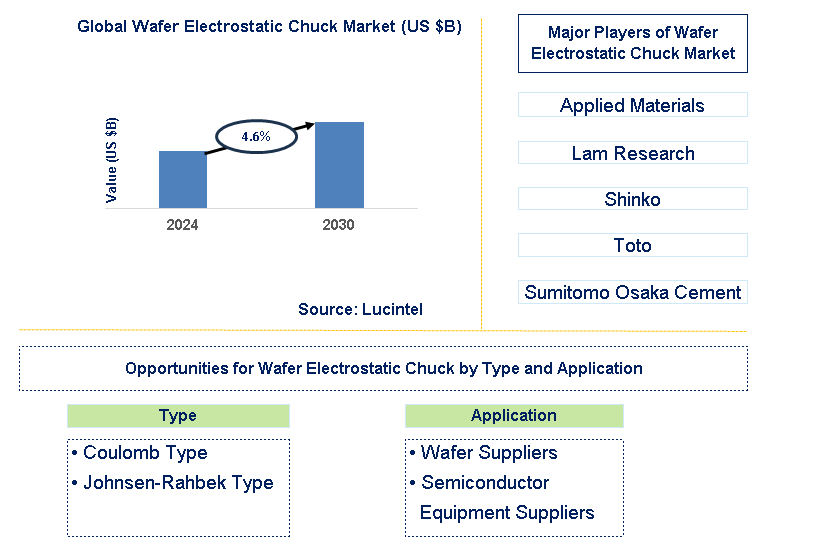
Key data points: The growth forecast = 4.6% annually for the next 6 years. Scroll below to get more insights. This market report covers trends, opportunities, and forecasts in the global wafer electrostatic chuck market to 2030 by type (coulomb type and johnsen-rahbek type), application (wafer suppliers and semiconductor equipment suppliers), and region (North America, Europe, Asia Pacific, and the Rest of the World)
We'll send your sample report shortly.
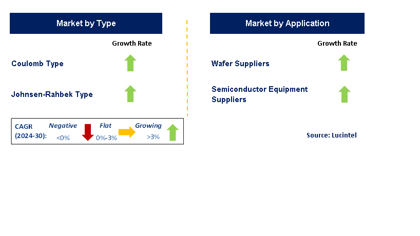
• Lucintel forecasts that, within the type category, coulomb type is expected to witness a higher growth over the forecast period.
• Within the application category, semiconductor equipment supplier is expected to witness a higher growth.
• In terms of regions, APAC is expected to witness highest growth over the forecast period. Gain valuable insight for your business decisions with our comprehensive 150+ page report
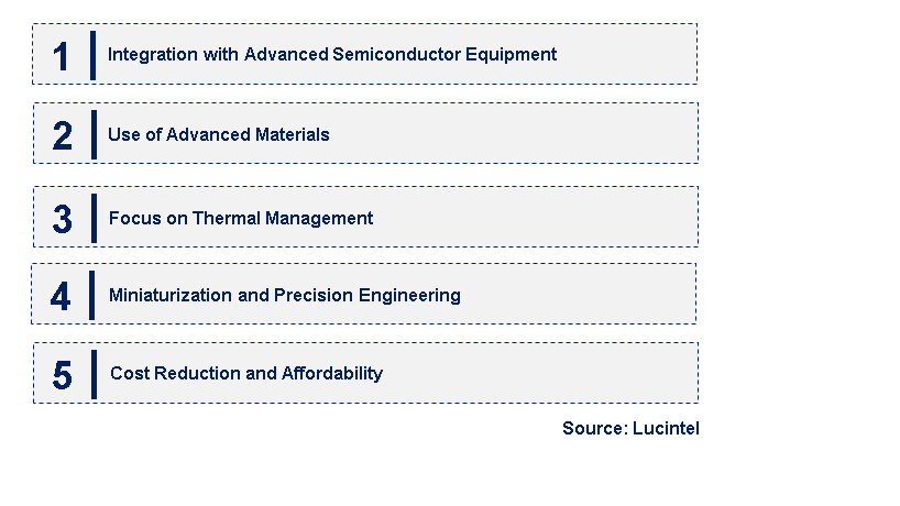
• Integration with Advanced Semiconductor Equipment: The integration of wafer electrostatic chucks with advanced semiconductor equipment is a key trend. This integration enhances precision and performance, supporting the manufacturing of more complex semiconductor devices. The trend reflects the industry's push toward greater miniaturization and higher performance in semiconductor production.
• Use of Advanced Materials: The adoption of advanced materials, such as ceramics and composites, is improving the performance of wafer electrostatic chucks. These materials offer better thermal stability, reduce contamination risks, and improve electrostatic control, contributing to higher yield and efficiency in semiconductor manufacturing processes.
• Focus on Thermal Management: Enhanced thermal management is becoming increasingly important in wafer electrostatic chuck design. Advanced cooling technologies and improved thermal dissipation techniques are being developed to manage heat more effectively, ensuring stable performance and preventing heat-related issues during semiconductor fabrication.
• Miniaturization and Precision Engineering: Miniaturization and precision engineering are driving the development of smaller and more accurate wafer electrostatic chucks. These advancements allow for more precise wafer handling and alignment, meeting the demands of advanced semiconductor processes that require higher levels of accuracy and control.
• Cost Reduction and Affordability: There is a growing focus on reducing the cost of wafer electrostatic chucks while maintaining performance and reliability. Cost-effective manufacturing processes and materials are being explored to make high-quality chucks more accessible to a broader range of semiconductor manufacturers, particularly in emerging markets. Emerging trends such as integration with advanced equipment, the use of advanced materials, a focus on thermal management, miniaturization, and cost reduction are reshaping the wafer electrostatic chuck market. These trends are driving improvements in performance, efficiency, and affordability, supporting the evolution of semiconductor manufacturing.
• Advanced Material Technologies: The introduction of advanced materials, such as high-performance ceramics and composites, has improved the thermal stability and electrostatic performance of wafer electrostatic chucks. These materials offer enhanced durability and reduce contamination risks, supporting higher precision and reliability in semiconductor manufacturing.
• Improved Thermal Management Solutions: New thermal management technologies have been integrated into wafer electrostatic chucks to better handle heat dissipation. Innovations such as advanced cooling systems and optimized heat sink designs help maintain stable performance and prevent overheating, addressing challenges in high-power semiconductor applications.
• Enhanced Electrostatic Control Mechanisms: Developments in electrostatic control mechanisms have led to more precise and stable wafer handling. Enhanced control algorithms and advanced electrostatic materials improve the accuracy of wafer alignment and gripping, contributing to higher yields and better performance in semiconductor production.
• Miniaturization of Design: The trend toward miniaturization has resulted in smaller, more compact wafer electrostatic chucks that are suitable for advanced semiconductor processes. These miniaturized designs offer improved precision and are compatible with next-generation manufacturing equipment, supporting the industry's push toward smaller and more complex devices.
• Cost-Effective Manufacturing Processes: Innovations in manufacturing processes have led to cost reductions for wafer electrostatic chucks. Advances in production techniques and material sourcing have made high-quality chucks more affordable, making them accessible to a broader range of semiconductor manufacturers and supporting market growth. Key developments such as advanced materials, improved thermal management, enhanced electrostatic control, miniaturization, and cost-effective manufacturing are driving improvements in the wafer electrostatic chuck market. These developments contribute to better performance, efficiency, and affordability, supporting the evolving needs of the semiconductor industry.
• Expansion into Emerging Markets: There is significant potential for growth in emerging markets where semiconductor manufacturing is expanding. Tailoring wafer electrostatic chuck solutions to meet local needs and addressing specific market requirements can capture new opportunities and drive market growth.
• Integration with Advanced Semiconductor Processes: The integration of wafer electrostatic chucks with advanced semiconductor processes, such as 5G and AI applications, presents growth opportunities. Developing chucks that meet the specific requirements of these high-tech processes can enhance performance and support technological advancements.
• Development of Next-Generation Materials: Investing in the development of next-generation materials for wafer electrostatic chucks can create growth opportunities. Advanced materials with improved performance characteristics can meet the demands of increasingly sophisticated semiconductor manufacturing processes and differentiate products in the market.
• Focus on Energy Efficiency: There is a growing emphasis on energy efficiency in semiconductor manufacturing. Wafer electrostatic chucks that incorporate energy-efficient technologies and contribute to reduced power consumption can appeal to manufacturers seeking to lower operational costs and improve sustainability.
• Customization for Specialized Applications: Offering customized solutions for specialized applications, such as high-precision and high-temperature environments, can provide growth opportunities. Tailoring wafer electrostatic chucks to meet specific industry needs can capture niche markets and address unique challenges. Strategic growth opportunities in the wafer electrostatic chuck market include expansion into emerging markets, integration with advanced processes, development of next-generation materials, a focus on energy efficiency, and customization for specialized applications. Leveraging these opportunities can drive innovation and market expansion.
• Technological Advancements: Advances in technology, such as improved materials and design innovations, drive the development of more efficient and reliable wafer electrostatic chucks. These advancements enhance performance and support the growing demands of semiconductor manufacturing.
• Growing Semiconductor Industry: The expanding semiconductor industry fuels demand for high-quality wafer electrostatic chucks. Increased production of advanced semiconductor devices requires precise and reliable wafer handling solutions to support higher yields and performance.
• Demand for Precision and Reliability: The need for higher precision and reliability in semiconductor manufacturing drives the adoption of advanced wafer electrostatic chucks. These chucks play a crucial role in ensuring accurate wafer alignment and handling, contributing to improved manufacturing outcomes.
• Focus on Miniaturization: The trend toward miniaturization in semiconductor devices creates demand for smaller and more precise wafer electrostatic chucks. Innovations in miniaturization support the production of increasingly complex and compact semiconductor components.
• Integration with Advanced Manufacturing Technologies: The integration of wafer electrostatic chucks with advanced manufacturing technologies, such as smart automation and AI, drives market growth. Enhanced functionality and compatibility with cutting-edge processes contribute to improved efficiency and performance. Challenges in the wafer electrostatic chuck market are:
• High Development Costs: The development of advanced wafer electrostatic chucks involves significant costs related to research, materials, and manufacturing. Balancing innovation with affordability can be challenging for both manufacturers and end-users.
• Complexity of Integration: Integrating new technologies and materials into existing systems can be complex. Ensuring compatibility and seamless operation requires extensive testing and development, which can be a barrier to adoption.
• Regulatory Compliance: Adhering to industry regulations and standards for semiconductor manufacturing can be challenging. Compliance with evolving regulations requires continuous updates and adjustments to products and processes. Major drivers such as technological advancements, industry growth, demand for precision, miniaturization, and integration with advanced technologies are shaping the wafer electrostatic chuck market. Challenges including high development costs, integration complexity, and regulatory compliance need to be addressed to capitalize on growth opportunities and ensure market success.
• Applied Materials
• Lam Research
• Shinko
• Toto
• Sumitomo Osaka Cement
• Mico
• Creative Technology
• Kyocera
• Entegris
• Krosaki Harima
• Coulomb Type
• Johnsen-Rahbek Type
• Wafer Suppliers
• Semiconductor Equipment Suppliers
• North America
• Europe
• Asia Pacific
• The Rest of the World
• United States: In the U.S., recent developments include advancements in the design and material composition of wafer electrostatic chucks aimed at enhancing their performance in high-precision semiconductor processes. Companies are focusing on improving thermal management and reducing contamination risks, driven by the increasing complexity of semiconductor devices and the push for higher yields in production.
• China: China is making significant strides in the wafer electrostatic chuck market by investing in local manufacturing capabilities and developing advanced technologies. Recent innovations include the integration of advanced materials and improved designs to support the growing semiconductor industry. The focus is also on cost reduction and enhancing reliability to compete with global standards.
• Germany: Germany's advancements in the wafer electrostatic chuck market are centered around precision engineering and material science. Recent developments include the introduction of new high-performance materials that offer better thermal stability and reduced electrostatic discharge. Germany's emphasis on quality and innovation supports its strong position in the high-tech semiconductor sector.
• India: In India, the wafer electrostatic chuck market is evolving with a focus on improving affordability and local manufacturing capabilities. Recent developments include the introduction of cost-effective solutions that cater to the growing semiconductor industry in India. Efforts are also being made to enhance the performance and reliability of electrostatic chucks to meet industry standards.
• Japan: Japan continues to lead in advanced wafer electrostatic chuck technologies, focusing on miniaturization and integration with next-generation semiconductor manufacturing equipment. Recent advancements include the development of chucks with enhanced electrostatic performance and improved thermal management to support the increasingly sophisticated needs of semiconductor fabrication.


• Applied Materials
• Lam Research
• Shinko
• Toto
• Sumitomo Osaka Cement
• Mico
• Creative Technology
• Kyocera
• Entegris
• Krosaki Harima Q5. Which wafer electrostatic chuck market segment will be the largest in future? Answer: Lucintel forecasts that coulomb type is expected to witness the higher growth over the forecast period. Q6. In wafer electrostatic chuck market, which region is expected to be the largest in next 5 years? Answer: In terms of regions, APAC is expected to witness highest growth over the forecast period. Q7. Do we receive customization in this report? Answer: Yes, Lucintel provides 10% customization without any additional cost.


Choose a license that fits your team. Instant PDF delivery.
Prices exclude taxes. Instant delivery. Custom licensing available on request.
Market Report · July 29, 2026
Market Report · July 20, 2026
Market Report · July 20, 2026
Trusted partner for strategic intelligence and business growth


Receive a complimentary market analysis tailored to your industry. Our analysts will identify key growth opportunities and competitive dynamics specific to your business.

Market size, growth rate, and key trend analysis for your specific sector.

Top competitor positioning and market share analysis.

Strategic recommendations backed by data-driven insights.
Get curated market intelligence and competitive moves straight to your inbox.
By subscribing, you agree to receive our monthly insights. Unsubscribe anytime.
Receive a complimentary market analysis tailored to your industry. Our analysts will identify key growth opportunities and competitive dynamics specific to your business.
Market size, growth rate, and key trend analysis for your specific sector.
Top competitor positioning and market share analysis.
Strategic recommendations backed by data-driven insights.
Get curated market intelligence, emerging trends, and competitive moves straight to your inbox each month.
By subscribing, you agree to receive our monthly insights. Unsubscribe anytime.
We'll send your sample report shortly.