
Market Report · July 29, 2026

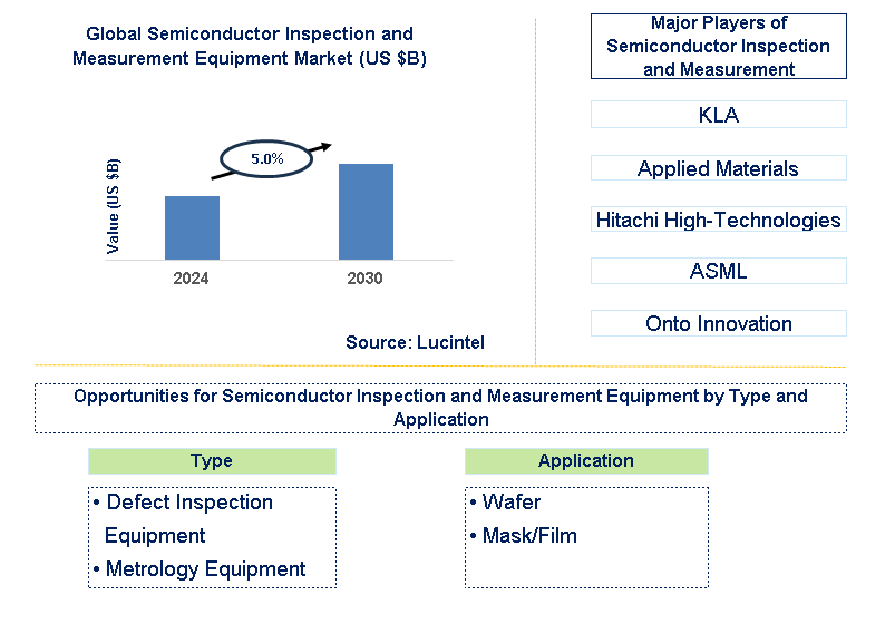
Key data points: The growth forecast = 5.0% annually for the next 6 years. Scroll below to get more insights. This market report covers trends, opportunities, and forecasts in the global semiconductor inspection and measurement equipment market to 2030 by type (defect inspection equipment and metrology equipment), application (wafer and mask/film), and region (North America, Europe, Asia Pacific, and the Rest of the World)
We'll send your sample report shortly.
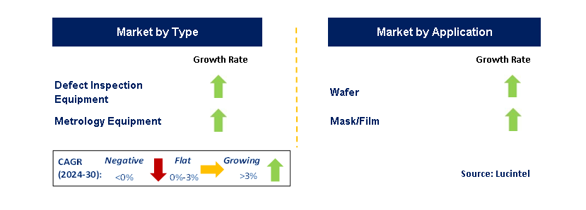
• Lucintel forecasts that, within the type category, defect inspection equipment is expected to witness higher growth over the forecast period because it is created to seek and detect any flaws or irregularities in semiconductors, guaranteeing that only devices free of flaws are manufactured.
• In terms of regions, APAC is expected to witness highest growth over the forecast period because of rise in outsourcing activities in the semiconductor industry, especially in countries like China and India. Gain valuable insights for your business decisions with our 150+ page report.
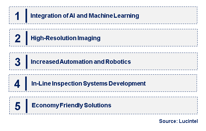
• Integration of AI and Machine Learning: AI and machine learning are increasingly integrated into inspection systems for enhancing defect detection and process optimization. These technologies enable real-time data analysis, improving accuracy and efficiency by identifying and addressing issues faster than traditional methods.
• High-Resolution Imaging: Increased demands from technology for miniaturization and complexity in semiconductor devices push the development of high-resolution imaging, driving advanced SEM and optical metrology. This provides greater insight into structures and aids in quality improvements.
• Increased Automation and Robotics: Automation and robotics are changing the way semiconductor inspections are carried out, increasing throughput times and maintaining higher consistency. Automated systems reduce human involvement, minimizing the possibility of human error and increasing inspection and measurement speed.
• In-Line Inspection Systems Development: In-line inspection systems are increasingly used, as they facilitate real-time monitoring during processing. These systems provide immediate feedback and adjustments to correct defects, ensuring efficiency in production.
• Cost-Effective Solutions: There is a growing emphasis on developing cost-effective inspection and measurement solutions that make advanced technologies more accessible. This aims to decrease production costs to expand the spread of sophisticated inspection tools across semiconductor manufacturing settings. These trends, such as the integration of AI, high-resolution imaging, automation, in-line inspection systems, and cost-effective solutions, shape the pace at which technology advances, promoting effectiveness and accuracy in semiconductor manufacturing processes.
• Advanced AI-Driven Inspection Systems: AI-powered inspection systems increase the effectiveness and efficiency of defect detection and analysis. With machine learning algorithms allowing for better pattern recognition and anomaly detection, AI-powered inspection systems lead to higher yields and less downtime.
• High-Resolution Metrology Tools: New high-resolution metrology tools provide very accurate measurements of semiconductor features, enabling the fabrication of small and complex devices while maintaining control over manufacturing processes.
• Improved Automation Technologies: Inspection processes now integrate automation technologies, increasing efficiency and consistency. Automated systems streamline operations, reduce human error, and accelerate inspection and measurement speeds, benefiting large-scale production.
• Real-Time In-Line Inspection Development: Real-time in-line inspection systems are rising for continuous monitoring during production. These systems offer immediate feedback, allowing on-the-fly adjustments to improve productivity and product quality.
• Cost-Effective Solutions: The focus is on developing cost-effective inspection and measurement solutions to spread advanced technologies. Efforts to reduce manufacturing costs and improve affordability support the use of these tools in semiconductor applications. Recent insights highlight the importance of AI-driven systems, high-resolution metrology, automation, real-time in-line inspection, and cost-effective solutions in enhancing inspection capabilities and supporting modern semiconductor manufacturing demands.
• Expanding Data Centers: As data centers expand, the demand for high-performance semiconductors rises, increasing the need for advanced inspection and measurement equipment to ensure hardware reliability and efficiency, driving strong growth opportunities.
• Advanced Memory Technology Development: New memory technologies like DRAM and NAND flash require precise inspection and measurement tools, opening opportunities for specialized equipment in advanced memory device fabrication.
• Growth in Automotive Electronics: The shift toward advanced electronics and autonomous vehicles in the automotive industry increases the demand for high-quality semiconductor components, requiring robust inspection systems to ensure reliability and safety.
• Advances in Consumer Electronics: The rapid growth of consumer electronics, including smartphones and wearables, has created significant opportunities for inspection and measurement equipment supporting semiconductor device manufacturing. High-precision tools are in demand to meet performance requirements.
• Focus on Emerging Semiconductor Materials: New semiconductor materials, such as wide-bandgap semiconductors, open new growth avenues for inspection and measurement equipment needed to analyze and validate the performance of advanced material systems. These strategic growth opportunities, including data center expansion, advanced memory technologies, automotive electronics, consumer electronics, and emerging semiconductor materials, will drive market growth and technological advancements to meet evolving semiconductor manufacturing needs.
• Technological Advances: Advances in technologies like AI and high-resolution imaging are driving market growth. These technologies increase precision and productivity in semiconductor manufacturing, supporting the creation of more complex devices.
• Increasing Demand for Semiconductor Devices: The rising demand in markets such as data centers, automotive, and consumer electronics has increased the need for inspection and measurement equipment, driving market expansion and innovation.
• Expanding Semiconductor Manufacturing Facilities: The global increase in semiconductor manufacturing facilities creates opportunities for advanced inspection and measurement equipment, as new facilities need the latest machinery to meet industry standards. Challenges in the market include:
• High Development and Manufacturing Costs: High costs associated with developing advanced inspection equipment hinder market growth, as companies must balance cost with competitive pricing.
• Complexity of Semiconductor Devices: The increasing complexity of semiconductor devices challenges inspection and measurement. More intricate designs drive continuous technological and methodological improvements to maintain accuracy and reliability.
• Regulatory and Compliance Issues: Vendors must navigate regulatory challenges and meet industry standards, requiring them to stay updated on changing regulations and certifications. Technological advances, rising demand, expanding manufacturing capacity, and device complexity are propelling the market, but high costs, complex devices, and regulatory issues remain challenges. Balancing these drivers and challenges is essential for market growth and technological progress.
• KLA
• Applied Materials
• Hitachi High-Technologies
• ASML
• Onto Innovation
• Lasertec
• SCREEN Semiconductor Solutions
• ZEISS
• Camtek
• Skyverse
• Defect Inspection Equipment
• Metrology Equipment
• Wafer
• Mask/Film
• North America
• Europe
• Asia Pacific
• The Rest of the World
• United States: Advanced inspection systems incorporating AI and machine learning are being developed to improve accuracy and speed. Companies like KLA and Applied Materials are introducing tools featuring real-time analysis and enhanced detection capabilities, crucial for the next wave of semiconductor manufacturing advancements.
• China: China is investing heavily to support its domestic industry. Local companies like SMIC and Naura are advancing automated inspection systems and optical metrology to improve yield rates and reduce production costs. This strategic push for self-sufficiency is driven by governmental initiatives.
• Germany: Germany remains focused on precision and automation in semiconductor inspection. Companies like Carl Zeiss and ASML are developing high-resolution imaging systems and advanced metrology tools aimed at improving quality and reliability in semiconductor devices.
• India: The Indian semiconductor inspection and measurement market is growing with increasing investments in technology and research. Indian companies and research institutions are developing affordable solutions and automation tools to support the country's expanding semiconductor manufacturing capabilities.
• Japan: Japan remains at the forefront of semiconductor inspection technology, with a focus on high-precision, high-output solutions. Companies like Nikon and Hitachi High-Technologies are innovating in electron microscopy and atomic force microscopy, which are critical for advanced semiconductor fabrication requirements.
• KLA
• Applied Materials
• Hitachi High-Technologies
• ASML
• Onto Innovation
• Lasertec
• SCREEN Semiconductor Solutions
• ZEISS
• Camtek
• Skyverse Q5. Which semiconductor inspection and measurement equipment market segment will be the largest in future? Answer: Lucintel forecasts that defect inspection equipment is expected to witness higher growth over the forecast period because it is created to seek and detect any flaws or irregularities in semiconductors, guaranteeing that only devices free of flaws are manufactured. Q6. In semiconductor inspection and measurement equipment market, which region is expected to be the largest in next 5 years? Answer: APAC is expected to witness highest growth over the forecast period because of rise in outsourcing activities in the semiconductor industry, especially in countries like China and India. Q.7 Do we receive customization in this report? Answer: Yes, Lucintel provides 10% customization without any additional cost.


Choose a license that fits your team. Instant PDF delivery.
Prices exclude taxes. Instant delivery. Custom licensing available on request.
Market Report · July 29, 2026
Market Report · July 20, 2026
Market Report · July 20, 2026
Trusted partner for strategic intelligence and business growth


Receive a complimentary market analysis tailored to your industry. Our analysts will identify key growth opportunities and competitive dynamics specific to your business.

Market size, growth rate, and key trend analysis for your specific sector.

Top competitor positioning and market share analysis.

Strategic recommendations backed by data-driven insights.
Get curated market intelligence and competitive moves straight to your inbox.
By subscribing, you agree to receive our monthly insights. Unsubscribe anytime.
Receive a complimentary market analysis tailored to your industry. Our analysts will identify key growth opportunities and competitive dynamics specific to your business.
Market size, growth rate, and key trend analysis for your specific sector.
Top competitor positioning and market share analysis.
Strategic recommendations backed by data-driven insights.
Get curated market intelligence, emerging trends, and competitive moves straight to your inbox each month.
By subscribing, you agree to receive our monthly insights. Unsubscribe anytime.
We'll send your sample report shortly.