
Market Report · July 22, 2026

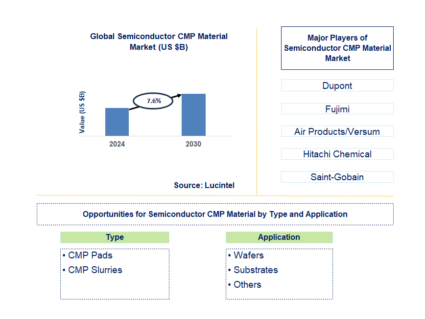
Key data points: The growth forecast = 7.6% annually for the next 6 years. Scroll below to get more insights. This market report covers trends, opportunities, and forecasts in the global semiconductor cmp material market to 2030 by type (CMP pads and CMP slurries), application (wafers, substrates, and others), and region (North America, Europe, Asia Pacific, and the Rest of the World)
We'll send your sample report shortly.
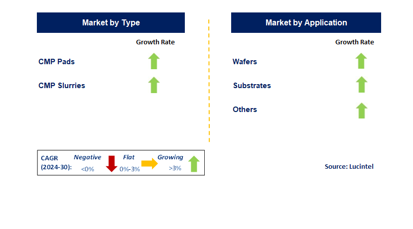
• Lucintel forecasts that, within the type category CMP pad is expected to witness higher growth over the forecast period.
• Within the application category, the wafer is expected to witness higher growth.
• In terms of regions, APAC is expected to witness the highest growth over the forecast period. A more than 150-page report is developed to help in your business decisions.
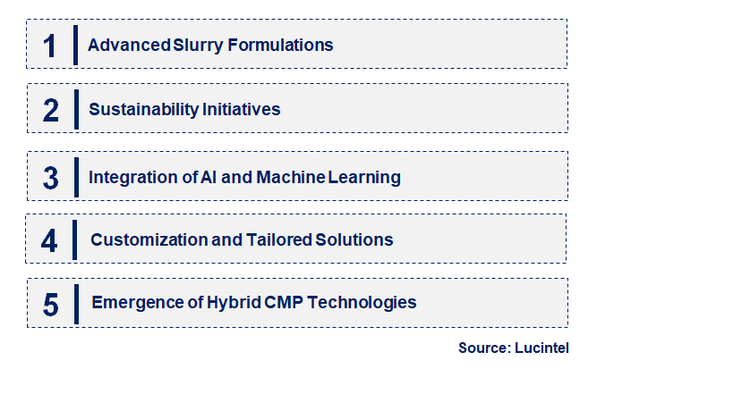
• Advanced Slurry Formulations: Recent innovations in slurry compositions are enabling higher removal rates and improved surface finishes. Manufacturers are experimenting with new chemical formulations that enhance the selectivity and efficiency of planarization processes. The use of nanomaterials and tailored additives has been shown to reduce defects and achieve better control over polishing rates. As semiconductor devices become more complex, the need for advanced slurries that can adapt to varying substrate materials is paramount, facilitating smoother integration into production lines.
• Sustainability Initiatives: The semiconductor industry is increasingly prioritizing sustainability, and CMP materials are no exception. Manufacturers are developing eco-friendly slurries and pads, focusing on reducing environmental impact during production and disposal. Innovations include biodegradable materials and reduced chemical usage, aligning with global efforts to minimize waste and carbon footprints. This trend is supported by regulatory pressures and the growing demand from consumers for sustainable practices, prompting companies to adopt greener technologies across their product lines.
• Integration of AI and Machine Learning: The adoption of artificial intelligence (AI) and machine learning (ML) technologies is transforming CMP processes. These tools are being used for real-time monitoring and optimization of CMP operations, leading to improved consistency and quality in wafer processing. Predictive analytics allow manufacturers to anticipate issues and minimize downtime, ultimately enhancing throughput and efficiency. This integration not only streamlines production but also fosters data-driven decision-making, crucial for adapting to the rapid changes in semiconductor manufacturing demands.
• Customization and Tailored Solutions: With the diverse requirements of various semiconductor applications, there is a growing trend toward customized CMP materials. Companies are increasingly focusing on developing tailored solutions that meet specific client needs, whether for advanced nodes or particular device architectures. This trend emphasizes the importance of collaboration between material suppliers and semiconductor manufacturers, leading to more effective and application-specific CMP processes. Customization ensures that manufacturers can achieve optimal results in planarization while minimizing defects and enhancing yield.
• Emergence of Hybrid CMP Technologies: Hybrid CMP technologies, which combine traditional mechanical polishing with advanced techniques, are gaining traction. These innovations aim to enhance the effectiveness of the planarization process while reducing surface damage. By integrating multiple methods, manufacturers can achieve better planarity and improved wafer quality. This trend is particularly significant as semiconductor devices become more intricate, requiring refined processes to meet stringent performance specifications. The rise of hybrid solutions indicates a shift toward more sophisticated manufacturing techniques in the CMP material market. These emerging trends are significantly reshaping the semiconductor CMP material market by driving innovation and addressing contemporary challenges. The focus on advanced materials, sustainability, and tailored solutions not only enhances efficiency but also aligns with the industry's commitment to responsible manufacturing practices. As the semiconductor landscape continues to evolve, these trends will play a pivotal role in ensuring that CMP processes keep pace with the demands of next-generation technologies, ultimately shaping the future of semiconductor fabrication.
• Advanced Slurry Formulations: Recent innovations in slurry formulations are enhancing the performance and efficiency of CMP processes. Manufacturers are introducing advanced chemical compositions that improve removal rates while minimizing defects on wafers. This includes the integration of nanoparticles and customized additives tailored for specific substrates. Such advancements allow for better control over polishing, which is essential as device geometries shrink. The ability to adjust slurry properties dynamically is becoming crucial for maintaining quality in high-volume manufacturing settings.
• Sustainability Initiatives: Sustainability is a major focus in recent CMP material developments. Companies are actively researching and developing eco-friendly slurries and pads that reduce the environmental impact of semiconductor manufacturing. This includes using biodegradable materials and reducing the use of harmful chemicals in production. Many manufacturers are also implementing recycling programs for CMP waste. These initiatives not only address regulatory pressures but also meet growing consumer demand for environmentally responsible practices in the semiconductor industry.
• Enhanced CMP Pad Materials: The development of new CMP pad materials has significantly improved polishing performance and lifespan. Innovations include the use of advanced polymer blends that offer superior durability and consistent performance over longer periods. These new pads provide better control over the polishing process, reducing wear and enhancing uniformity across the wafer. Additionally, manufacturers are focusing on developing pads that can be easily cleaned and reused, contributing to both cost savings and sustainability efforts in semiconductor fabrication.
• AI-Driven Process Optimization: The integration of artificial intelligence (AI) in CMP processes is revolutionizing manufacturing efficiency. AI-driven tools are being used to monitor and optimize CMP operations in real-time, allowing for immediate adjustments to improve quality and yield. Predictive analytics help identify potential issues before they arise, reducing downtime and waste. This technological advancement is transforming data into actionable insights, making the CMP process more adaptive and responsive to changing production requirements.
• Hybrid CMP Technologies: Hybrid CMP technologies that combine mechanical and chemical polishing methods are gaining traction. These systems are designed to enhance the effectiveness of planarization while minimizing damage to sensitive wafer surfaces. By integrating different polishing techniques, manufacturers can achieve superior results in terms of planarity and defect reduction. This development is particularly important for advanced semiconductor devices, which require precise manufacturing processes to meet stringent performance specifications. These recent developments are significantly impacting the semiconductor CMP material market by enhancing efficiency, sustainability, and overall performance. As the demand for advanced semiconductor technologies continues to rise, these innovations are essential for meeting the challenges of modern fabrication processes. The ongoing improvements in CMP materials and techniques are not only driving production efficiencies but are also aligning with industry-wide efforts to adopt more sustainable practices, setting the stage for future growth and innovation.
• Consumer Electronics: The consumer electronics sector is experiencing rapid growth, driven by the demand for smaller, more powerful devices. This trend creates significant opportunities for CMP materials that cater to advanced semiconductor manufacturing. Innovations in slurries and pads tailored for high-density chips can enhance performance and reduce production costs. As devices become more intricate, manufacturers will seek CMP solutions that offer better planarity and defect control, opening avenues for specialized product offerings and collaborations.
• Automotive Electronics: With the automotive industry increasingly incorporating advanced electronics, there is a substantial growth opportunity in CMP materials tailored for automotive applications. The demand for high-performance semiconductors in electric vehicles and autonomous driving systems is on the rise. CMP solutions that ensure reliability and durability under extreme conditions will be critical. Manufacturers can leverage this opportunity by developing specialized CMP materials that meet the stringent safety and performance standards required in the automotive sector.
• High-Performance Computing (HPC): The HPC sector is expanding rapidly, fueled by the need for advanced processing power in data centers and cloud computing. This growth presents opportunities for CMP materials that enhance the performance and efficiency of chips used in servers and supercomputers. As HPC devices evolve, the demand for specialized slurries that improve yield and reduce defects becomes essential. Companies can focus on R&D to develop high-performance CMP solutions that cater to the specific needs of this demanding application.
• Telecommunications and 5G Technologies: The rollout of 5G technology and telecommunications infrastructure is driving demand for high-frequency semiconductors. CMP materials that facilitate the manufacturing of these advanced chips will be critical for meeting market needs. Growth opportunities exist in developing slurries that optimize signal integrity and reduce loss in high-frequency applications. Companies can invest in innovations that specifically address the challenges of manufacturing 5G components, positioning themselves as key players in this growing market segment.
• Artificial Intelligence and Machine Learning Applications: As AI and machine learning technologies become integral to various sectors, the semiconductor industry must adapt to support these applications. The demand for specialized CMP materials that enable efficient processing in AI chips is rising. Opportunities exist for developing tailored CMP solutions that enhance performance and yield for AI-related semiconductor devices. Companies can capitalize on this trend by focusing on R&D to create advanced materials that meet the unique requirements of AI applications, ensuring their competitiveness in this expanding market. These strategic growth opportunities across key applications in the semiconductor CMP material market highlight the potential for innovation and development. By focusing on tailored solutions that meet the specific needs of diverse sectors, stakeholders can enhance their market presence and drive growth. As the semiconductor landscape evolves, leveraging these opportunities will be crucial for companies aiming to maintain a competitive edge and contribute to the industry’s advancement.
• Technological Advancements: Rapid advancements in semiconductor technologies, such as the transition to smaller nodes (e.g., 5nm, 3nm), are a significant driver for the CMP materials market. As devices become more complex, the demand for high-performance CMP solutions that can achieve better surface finishes and reduce defects is growing. Innovations in slurry formulations and pad materials are critical to meeting these new technical requirements. Companies that invest in R&D to develop advanced CMP solutions can gain a competitive edge, positioning themselves as leaders in an increasingly demanding market.
• Increased Demand for Miniaturization: The ongoing trend toward miniaturization in electronics drives the need for advanced CMP materials. As manufacturers strive to produce smaller, more efficient chips, the requirements for planarization become more stringent. CMP processes are essential for achieving the precision needed in modern semiconductor devices. This trend opens up opportunities for suppliers to develop specialized materials that cater to the specific needs of miniaturized components, thereby enhancing yield and performance in production processes.
• Growth of Emerging Technologies: Emerging technologies, such as 5G, AI, and IoT, are significantly driving the demand for semiconductors, subsequently boosting the CMP material market. As these technologies require more advanced chips, manufacturers need CMP solutions that can effectively handle the unique challenges associated with high-frequency and high-performance applications. The expansion of these sectors creates new opportunities for innovation and growth in CMP materials, pushing manufacturers to develop specialized solutions that address specific requirements.
• Sustainability Trends: The increasing emphasis on sustainability and eco-friendly practices is reshaping the CMP materials market. As manufacturers and consumers alike become more conscious of environmental impacts, there is a growing demand for sustainable CMP solutions, including biodegradable slurries and pads with reduced chemical footprints. Companies that adopt sustainable practices can enhance their brand reputation and appeal to environmentally conscious clients. This trend not only encourages innovation in material formulations but also aligns with regulatory pressures for more responsible manufacturing processes.
• Economic Growth in Key Regions: Economic growth in regions such as Asia-Pacific, particularly China and India, is driving investment in semiconductor manufacturing capabilities. This growth translates into increased demand for CMP materials as new fabs are built and existing ones are upgraded. As these regions expand their semiconductor ecosystems, the need for advanced CMP solutions becomes more pronounced, presenting significant opportunities for manufacturers. Companies that strategically position themselves in these growing markets can benefit from increased sales and market share. Challenges in the Semiconductor CMP Material Market:
• Supply Chain Disruptions: Supply chain challenges, exacerbated by global events such as the COVID-19 pandemic, pose a significant risk to the CMP materials market. Fluctuations in the availability of raw materials can lead to increased production costs and delays in delivery timelines. Manufacturers may struggle to meet the rising demand for CMP solutions if supply chains remain unstable. Addressing these challenges requires companies to enhance their supply chain resilience and consider diversifying suppliers to mitigate risks.
• Regulatory Compliance: The semiconductor industry faces stringent regulatory requirements related to environmental protection and chemical usage. Compliance with these regulations can create challenges for CMP material manufacturers, particularly in the development of sustainable products. Meeting these standards often requires additional investment in R&D and process adjustments, which can impact profit margins. Companies must stay informed about evolving regulations and adapt their product offerings accordingly to avoid potential penalties and maintain market access.
• Intense Market Competition: The CMP materials market is characterized by intense competition among established players and new entrants. This competition can lead to pricing pressures, making it challenging for companies to maintain profitability while investing in innovation. Additionally, rapid technological changes mean that companies must continually adapt to stay relevant. Firms need to differentiate their products through unique value propositions, such as superior performance or sustainability features, to remain competitive in a crowded marketplace. The interplay of drivers and challenges in the semiconductor CMP material market significantly shapes its trajectory. While technological advancements and growing demand for miniaturization and sustainability present substantial growth opportunities, challenges such as supply chain disruptions and intense competition must be effectively managed. Stakeholders that can navigate these complexities while leveraging market drivers will be better positioned to capitalize on emerging trends and maintain a competitive edge in the evolving semiconductor landscape. The ability to adapt to changing conditions will ultimately determine success in this dynamic market.
• Dupont
• Fujimi
• Air Products/Versum Material
• Hitachi Chemical
• Saint-Gobain
• Asahi Glass
• Ace Nanochem
• CMP Pads
• CMP Slurries
• Wafers
• Substrates
• Others
• North America
• Europe
• Asia Pacific
• The Rest of the World
• United States: Recent developments in the U.S. semiconductor CMP market focus on novel slurry formulations that improve defectivity and surface finish. Companies are investing in AI-driven process optimization to enhance throughput and reduce costs. Additionally, advancements in CMP pad materials, such as the introduction of new polymer blends, have led to better pad life and uniformity. Collaborations between semiconductor manufacturers and research institutions are driving innovation, particularly in sustainability efforts, where eco-friendly CMP materials are being explored.
• China: In China, the CMP material market has seen rapid growth due to its expanding semiconductor industry. Key advancements include the development of proprietary slurry technologies that cater specifically to local manufacturers' needs. Chinese firms are increasingly focusing on reducing dependence on foreign suppliers by enhancing domestic production capabilities. Moreover, investments in research and development are leading to innovations in high-performance CMP pads, aimed at achieving better planarity and reduced wear. The government’s support for semiconductor self-sufficiency is further accelerating these developments.
• Germany: Germany has emerged as a leader in the CMP materials sector, emphasizing high-precision applications for automotive and industrial semiconductors. Recent innovations include the integration of nanomaterials into CMP slurries to achieve superior planarization results. German companies are also pioneering sustainable practices, such as developing biodegradable CMP materials. The collaboration between universities and industry is fostering breakthroughs in CMP technology, particularly for advanced nodes. Additionally, a strong focus on quality control and process stability is shaping the future of CMP in the German semiconductor landscape.
• India: In India, the CMP material market is experiencing growth fueled by its burgeoning semiconductor ecosystem. Recent developments focus on localizing slurry and pad production to meet the demands of domestic fabs. Indian companies are innovating in low-cost CMP solutions while improving performance metrics like removal rates and surface quality. Research initiatives are being launched to explore the use of alternative materials in CMP processes, aimed at enhancing sustainability. As the government promotes semiconductor manufacturing, advancements in CMP materials are becoming increasingly critical for local players.
• Japan: Japan continues to be at the forefront of semiconductor CMP innovations, leveraging its advanced manufacturing expertise. Recent developments include the refinement of advanced slurry formulations that enhance the performance of next-generation semiconductor devices. Japanese firms are also leading the way in developing hybrid CMP pads that optimize both polishing efficiency and durability. The integration of smart technologies in CMP processes is gaining traction, allowing for real-time monitoring and adjustment. Furthermore, Japan's focus on precision engineering ensures that its CMP materials meet the stringent requirements of high-end applications.


• Dupont
• Fujimi
• Air Products/Versum Material
• Hitachi Chemical
• Saint-Gobain
• Asahi Glass
• Ace Nanochem Q5. Which semiconductor CMP material market segment will be the largest in future? Answer: Lucintel forecasts that CMP pad is expected to witness higher growth over the forecast period. Q6. In semiconductor CMP material market, which region is expected to be the largest in next 5 years? Answer: APAC is expected to witness the highest growth over the forecast period. Q.7 Do we receive customization in this report? Answer: Yes, Lucintel provides 10% customization without any additional cost.


Choose a license that fits your team. Instant PDF delivery.
Prices exclude taxes. Instant delivery. Custom licensing available on request.
Market Report · July 22, 2026
Market Report · July 22, 2026
Market Report · July 22, 2026
Trusted partner for strategic intelligence and business growth


Receive a complimentary market analysis tailored to your industry. Our analysts will identify key growth opportunities and competitive dynamics specific to your business.

Market size, growth rate, and key trend analysis for your specific sector.

Top competitor positioning and market share analysis.

Strategic recommendations backed by data-driven insights.
Get curated market intelligence and competitive moves straight to your inbox.
By subscribing, you agree to receive our monthly insights. Unsubscribe anytime.
Receive a complimentary market analysis tailored to your industry. Our analysts will identify key growth opportunities and competitive dynamics specific to your business.
Market size, growth rate, and key trend analysis for your specific sector.
Top competitor positioning and market share analysis.
Strategic recommendations backed by data-driven insights.
Get curated market intelligence, emerging trends, and competitive moves straight to your inbox each month.
By subscribing, you agree to receive our monthly insights. Unsubscribe anytime.
We'll send your sample report shortly.