
Market Report · May 18, 2026

This market report covers trends, opportunities, and forecasts in the global materials for next-generation lithography market to 2031 by technology (photoresist material and ancillary material), end use industry (automotive, consumer electronics, it & telecommunications, and others), and region (North America, Europe, Asia Pacific, and the Rest of the World)
We'll send your sample report shortly.
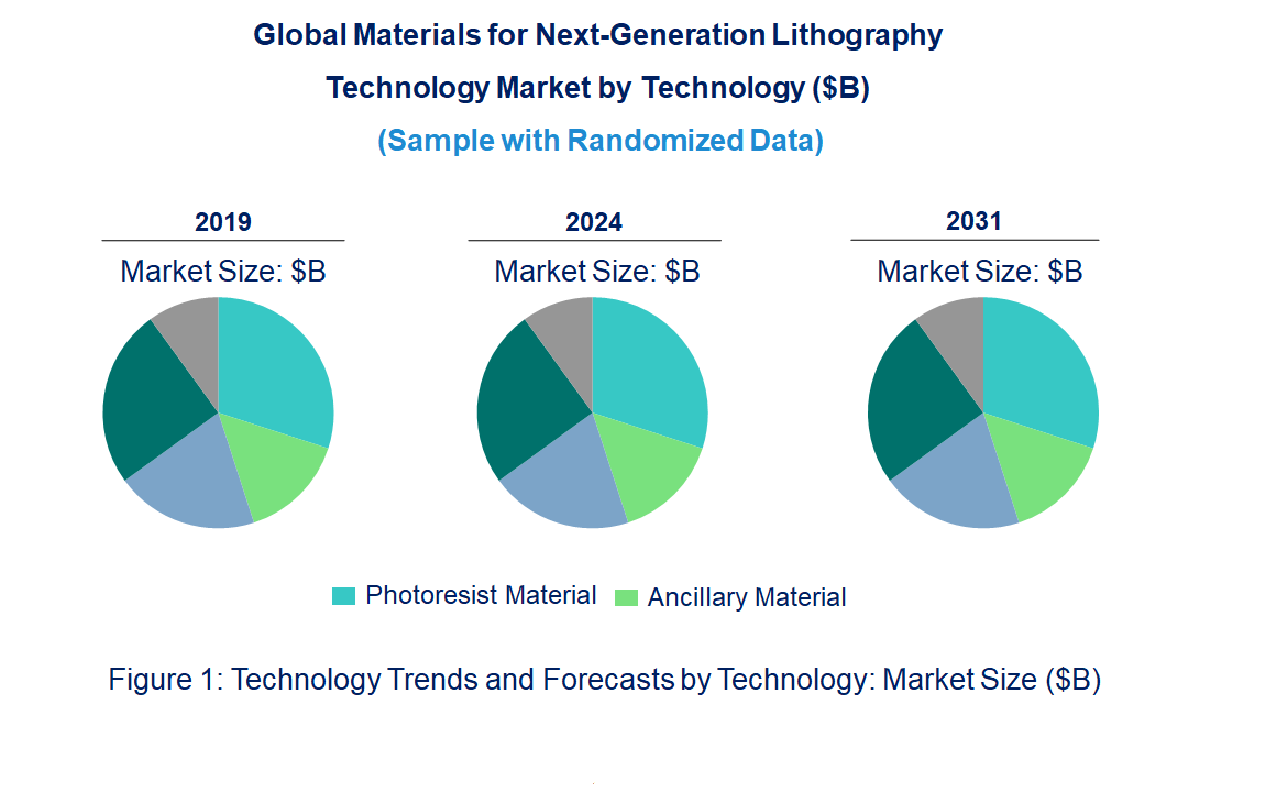
![Materials For Next-Generation Lithography Market Trend and Forecast by End Use Industry [Value from 2019 to 2031]:](https://lucintel.com/images/Materials-for-Next-Generation-Lithography-Technology-Market-Segment.png "Materials For Next-Generation Lithography Market Trend and Forecast by End Use Industry [Value from 2019 to 2031]:")
• Transitioning towards EUV Lithography: EUV lithography is becoming the industry standard for advanced semiconductor manufacturing. Using wavelengths as short as 13.5 nm, EUV allows for much smaller features and denser chip designs, which are so important for AI applications needing high performance and processing power.
• Adoption of High-Resolution Photoresists: The advanced photoresists that may show high-resolution capabilities under EUV light enhance precision and scalability in next-gen chips. These materials allow more intricate patterns, which thereby improve the performance and efficiency of AI chips.
• Nanoparticle-based Materials: Nanoparticles are now being introduced in lithographic processes to get finer patterns and to achieve the accuracy of feature replication. These materials assist in developing chips with higher transistor densities, which are critical for AI workloads requiring rapid processing capabilities.
• Hybrid Lithography Techniques: Hybrid approaches are more commonly being used, which involve combining EUV with multiple patterning techniques. This helps in overcoming the constraints posed by EUV for smaller node sizes and allows AI chips to have better performance as they can have more complex circuit designs at lower costs.
• Alternative Materials for Lithography Development: New alternatives to traditional photoresists, such as nanoimprint lithography (NIL) resins and high-performance dielectrics, are being explored for potential application. These new materials can enable lithography to reach its limit, to push the speed and low-cost production of AI-centric chips with higher capabilities. The continued evolution of materials for next-generation lithography is reshaping the AI semiconductor market. Trending on this are the switch to EUV, photoresist development at ever-high resolutions, and hybrid and alternative material adoptions. They are empowering the creation of more powerful, efficient, and scalable chips, in turn playing a critical role in keeping up with the accelerating demands of AI technologies and powering advancements in AI performance within industries.
• TOK: has developed its EUV (Extreme Ultraviolet) photoresists, which are critical for manufacturing smaller, more powerful chips. The latest resists from TOK are formulated to provide higher resolution and better process stability, which directly translates to higher throughput and yield in semiconductor fabrication. Innovation is key to supporting production at 5nm and beyond.
• JSR: It has been working towards improvement in the quality of photoresist materials, trying to improve EUV lithography. The company has announced newer, more advanced resists that yield higher resolution, better etch resistance, and lower defectivity. The joint work of the company with leading integrated device manufacturers helped optimize EUV technology efficiency for production processes. This will allow even more compact, efficient processors for AI.
• DuPont is working on next-generation materials that include advanced photoresists and etching materials compatible with EUV lithography. Their inventions help to address the challenges in patterning at extremely small scales, especially in the formation of ultra-thin films that are crucial for next-generation semiconductors. Process optimization by DuPont is also improving throughput and yield.
• Shin-Etsu Chemical: It has achieved success in advanced material manufacturing for semiconductor fabrication, particularly in silicon wafer manufacturing. High-purity chemical solutions provided by Shin-Etsu are supporting the enhancement of lithography process efficiency through improved surface quality and reduced defects, an imperative factor for sustaining semiconductor fabrication yields at a high level.
• Fujifilm: It has been diversifying its portfolio of photoresist materials for both EUV and traditional deep ultraviolet (DUV) lithography. The company has developed new resists that provide better resolution and resistance to post-lithography etching processes. These developments are crucial to enable the mass production of smaller chips used in AI and high-performance computing.
• Sumitomo Chemica: Itl has been working on the development of advanced photoresists that have better pattern fidelity and lower defect rates in EUV processes. Their resists are designed to improve the production of smaller semiconductor nodes, addressing challenges such as line-edge roughness and pattern collapse, both of which are significant hurdles in nanometer-scale chip fabrication.
• Allresist: lt has been pushing the boundaries of resist technology by offering materials that are optimized for sub-7nm node production. Their developments in negative and positive tone resists for both EUV and DUV lithography are helping semiconductor manufacturers improve the resolution and uniformity of critical layers, leading to higher yield rates in the production of next-gen chips.
• Micro Resist Technology: It has developed high-performance resists for both EUV and DUV lithography, targeting the fabrication of semiconductor nodes at 5nm and beyond. Their resists are designed for improved resolution and higher etch resistance, which helps to maintain high levels of precision during the lithography process, thereby producing increasingly smaller and more powerful chips.
• Merck: It has been advancing the materials for EUV lithography, including photoresists and other supporting chemicals such as antireflective coatings and hard masks. Their contributions are assisting in overcoming the challenges linked with high-resolution imaging and defectivity at the 3nm node and beyond that supporting the growth of AI hardware and next-gen chips.
• Dongjin Semichem: It has been aggressively investing in developing high-performance materials, which have mainly focused on photoresists and etching agents to enhance the resolution and precision for patterning needed for semiconductor nodes at sub-5nm. Dongjin is, therefore, supporting semiconductor makers to maintain yield and performance through enhanced process stability and defect reduction. These developments in materials for next-generation lithography are critical in the advancements of semiconductor manufacturing technologies for progressively smaller, faster, and lower-power chips. As these companies advance in innovation, their contribution is very important to the ever-advancing AI hardware and next-generation technologies.
• Advanced AI Hardware Demand: The growth of AI and machine learning is pushing the demand for advanced semiconductor chips, which calls for innovative materials for lithography. These materials allow for smaller transistors, greater processing power, and energy efficiency, all of which are necessary for the next generation of AI processors.
• EUV Lithography: EUV lithography is enabling the production of chips with smaller nodes, allowing for more powerful AI chips. This advance has driven demand for advanced photoresists and materials that can support these processes, driving innovation and improving chip performance.
• Technological Advancements in Nanotechnology: Materials science evolves along with AI. Nanomaterials research helps advance lithography technology, making it possible to develop more precise materials that improve chip design, reduce defects, and enhance the overall performance of AI hardware. Challenges:
• High Production Costs: Next-gen lithography materials, like EUV photoresists, are expensive to develop and produce. The high production costs put this technology out of reach for many companies, thereby limiting access to leading-edge semiconductor manufacturing.
• Material Defects and Yield Issues: As transistor sizes reduce, patterning requires high accuracy. Material defects and low yield during production contribute to higher costs and efficiency reduction in chip manufacturing for semiconductor fabrication; thus, scaling up AI chips becomes a significant challenge. The technological advancements in semiconductor manufacturing increasingly push regulatory challenges regarding environmental effects as well as safety. Sophisticated materials used within these lithography processes have added much more complication to the production process owing to the need for tighter compliance with environmental standards in regards to development and disposal
• Low-Cost, High-Performance Materials: One of the key opportunities is the research that is going on in low-cost photoresists and other materials that maintain high performance. Innovation in this area could cut production costs and make advanced semiconductor technologies more accessible, which would promote further adoption of AI hardware.
• Collaboration and Partnerships Among Key Players: The collaboration between semiconductor manufacturers, materials suppliers, and research institutions will be the source of breakthroughs in lithography materials. By pooling resources and knowledge, these partnerships can overcome challenges related to defects, yield issues, and material efficiency.
• Improvements in Lithography Equipment and Technology: Improvements in the equipment and techniques used in lithography, including EUV machines, are an opportunity. Enhanced lithography equipment, improving resolution and reducing defects, would directly help the development of AI processors and accelerate the production of next-gen chips. The growths in the materials for next-generation lithography technology in the AI technology market are based on its opportunities in future outcomes. Despite the obstacles facing materials with high production costs and defects, as well as regulatory issues, advances are being made in materials through research and development, mutual collaborations, and the development and improvement of lithography technologies. These are significant elements for demand increases in advanced AI chips. They also drive forward new AI technology.
• Tokyo Ohka Kogyo
• JSR
• Dupont De Nemours
• Shin-Etsu Chemical
• Fujifilm
• Sumitomo Chemical
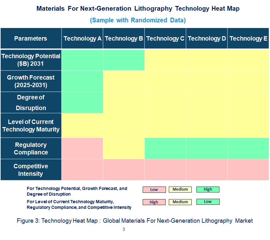
• Technology Readiness by Technology Type and Key Applications: Photoresist materials, especially for EUV lithography, are highly mature. Leading-edge materials are already supporting semiconductor nodes as small as 5nm. Their primary applications are in the production of advanced microchips used in AI, consumer electronics, and high-performance computing. Ancillary materials such as antireflective coatings, etchants, and solvents are equally important, improving the accuracy of patterning in lithography. These materials are ready for mass production, with primary applications across semiconductor manufacturing, from memory devices to processors. Both of these technologies are essential to continue scaling down transistors and developing next-generation technologies such as AI processors and 5 G.
• Disruption Potential by Technology Type: There is significant disruption potential for photoresist materials and ancillary materials in semiconductor manufacturing. Photoresists, especially those used in EUV (extreme ultraviolet) lithography, allow for smaller, more efficient chips. The continued development of these materials propels the advancement of Moore’s Law, which will then enable the creation of next-generation AI processors and quantum computing hardware. Ancillary materials like etching agents, antireflective coatings, and solvents are also important for enhancing chip yield and resolution. The improvements in these materials can greatly reduce production costs, improve chip performance, and help transition to smaller nodes. They can thus revolutionize industries based on cutting-edge technology.
• Competitive Intensity and Regulatory Compliance: The competitive intensity in the photoresist and ancillary material markets is high, with leading players like Tokyo Ohka Kogyo, JSR, and DuPont constantly pushing the envelope in terms of innovation and high-performance solutions for semiconductor makers. Companies must continuously invest in R&D to stay ahead in terms of emerging technology and market trends. Also, the company has to adhere to very stringent environmental, health, and safety regulations. This encompasses adherence to international guidelines in chemical safety, material disposal, and manufacturing practices. Companies also face hurdles to sustainability compliance in the absence of detrimental impacts on performance, with alternatives that are more environmentally friendly.
• Photoresist Material
• Ancillary Material
• Automotive
• Consumer Electronics
• IT & Telecommunications
• Others
• North America
• Europe
• Asia Pacific
• The Rest of the World
• Latest Developments and Innovations in the Materials For Next-Generation Lithography Technologies
• Companies / Ecosystems
• Strategic Opportunities by Technology Type


Choose a license that fits your team. Instant PDF delivery.
Prices exclude taxes. Instant delivery. Custom licensing available on request.
Market Report · May 18, 2026
Market Report · May 18, 2026
Market Report · May 18, 2026
Trusted partner for strategic intelligence and business growth


Receive a complimentary market analysis tailored to your industry. Our analysts will identify key growth opportunities and competitive dynamics specific to your business.

Market size, growth rate, and key trend analysis for your specific sector.

Top competitor positioning and market share analysis.

Strategic recommendations backed by data-driven insights.
Get curated market intelligence and competitive moves straight to your inbox.
By subscribing, you agree to receive our monthly insights. Unsubscribe anytime.
Receive a complimentary market analysis tailored to your industry. Our analysts will identify key growth opportunities and competitive dynamics specific to your business.
Market size, growth rate, and key trend analysis for your specific sector.
Top competitor positioning and market share analysis.
Strategic recommendations backed by data-driven insights.
Get curated market intelligence, emerging trends, and competitive moves straight to your inbox each month.
By subscribing, you agree to receive our monthly insights. Unsubscribe anytime.
We'll send your sample report shortly.