
Market Report · July 29, 2026

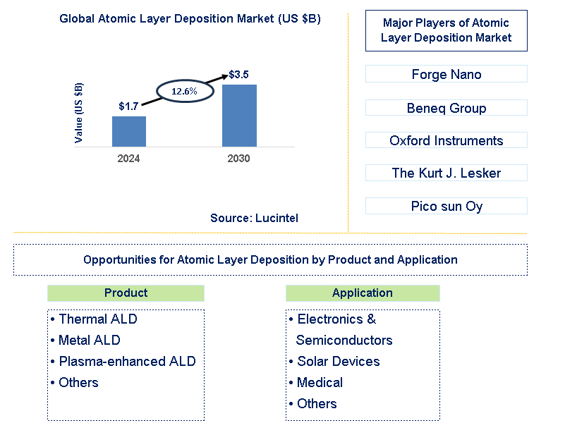
Key data points: The market size in 2030 = $3.5 billion, growth forecast = 12.6% annually for the next 6 years. Scroll below to get more insights. This market report covers trends, opportunities, and forecasts in the global atomic layer deposition market to 2030 by product (thermal ALD, metal ALD, plasma-enhanced ALD, and others), application (electronics & semiconductors, solar devices, medical, and others), and region (North America, Europe, Asia Pacific, and the Rest of the World)
We'll send your sample report shortly.
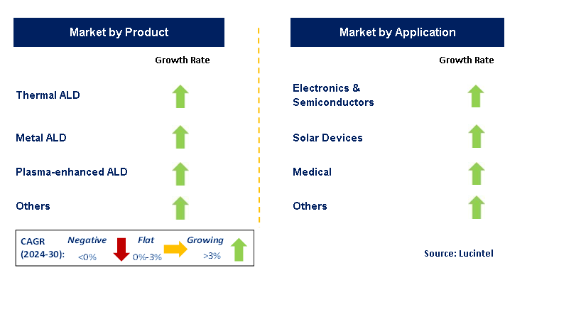
• Lucintel forecasts that, within the product category, thermal ALD will remain the largest segment over the forecast period due to regardless of the surface shape, this kind of atomic layer deposition process creates uniform layers with surface control and conformance.
• Within the application category, electronics & semiconductor will remain the largest segment due to rising semiconductor demand is expected to drive the market for atomic layer deposition, which will benefit from the growing need for electronic components in the automotive sector.
• APAC will remain the largest region over the forecast period due to a higher level of government investment in infrastructure development to entice leading car and electronics companies to establish production plants in the region. Gain valuable insight for your business decisions with our comprehensive 150+ page report
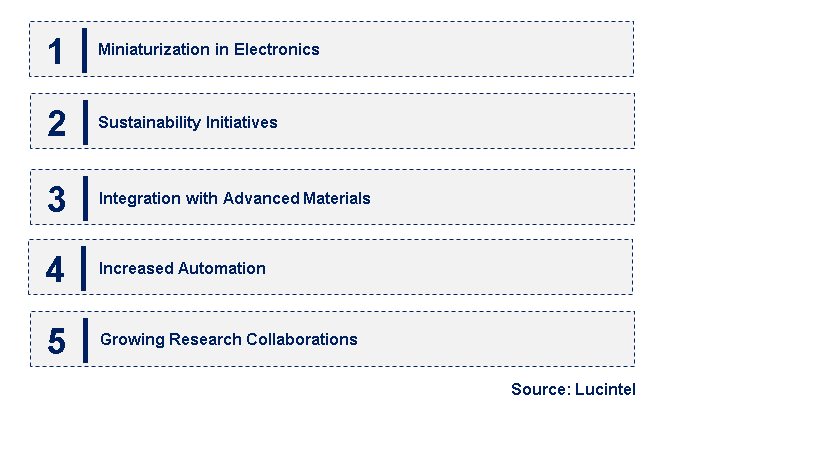
• Miniaturization in Electronics: The trend toward miniaturization in the electronics industry is driving demand for ALD technologies. As devices become smaller and more complex, ALD provides precise control over thin-film deposition, enabling the production of advanced components that meet stringent performance criteria.
• Sustainability Initiatives: Growing environmental concerns are pushing manufacturers to adopt sustainable practices in ALD processes. This includes developing eco-friendly precursors and waste reduction strategies, allowing companies to enhance their sustainability profiles while meeting regulatory requirements.
• Integration with Advanced Materials: The integration of ALD with novel materials, such as two-dimensional materials and nanomaterials, is expanding application areas. This trend allows for creating advanced electronic devices, sensors, and energy storage solutions, driving innovation across multiple sectors.
• Increased Automation: The shift toward automation in ALD processes is improving efficiency and consistency. Automated systems enable manufacturers to scale production while minimizing human error, leading to higher-quality thin films and reducing overall production costs.
• Growing Research Collaborations: Increased collaboration between academia and industry is fostering innovation in ALD technologies. These partnerships are leading to breakthroughs in process development and material discovery, driving advancements in ALD applications across various industries. These emerging trends are reshaping the atomic layer deposition market by fostering innovation, enhancing sustainability, and expanding application areas, ultimately driving growth and transformation in the industry.
• Advanced ALD Equipment: Companies are investing in next-generation ALD equipment that enhances deposition rates and improves film uniformity. These advancements enable more efficient production processes, facilitating broader applications in semiconductor manufacturing and materials science.
• Innovative Precursors: The development of novel precursors is enhancing the range of materials that can be deposited using ALD. These innovative precursors improve the quality and performance of thin films, expanding their applicability in advanced electronics and energy devices.
• Sustainable Practices: Manufacturers are adopting sustainable practices by developing eco-friendly precursors and optimizing processes to reduce waste. This shift aligns with growing environmental regulations and consumer preferences, enhancing the sustainability profile of ALD technologies.
• Expanded Application Areas: ALD is being applied in new sectors, such as biomedicine and optics, due to its unique capabilities in depositing thin films with precision. This expansion into diverse applications is driving market growth and innovation.
• Collaborative Research Initiatives: Increased collaboration between research institutions and industry players is accelerating advancements in ALD technology. These partnerships foster innovation and help translate research breakthroughs into practical applications, enhancing market competitiveness. These developments are significantly impacting the atomic layer deposition market by enhancing efficiency, promoting sustainability, and expanding application areas, ultimately driving growth and innovation across the industry.
• Semiconductor Manufacturing: The semiconductor industry is a key growth area for ALD, driven by the need for advanced materials and precise deposition techniques. As device architectures become more complex, ALD provides the control necessary for producing high-performance components.
• Energy Storage Solutions: The demand for efficient energy storage solutions, particularly in batteries and supercapacitors, is driving the adoption of ALD technologies. ALD can create high-quality coatings that enhance battery performance, making it an attractive option for manufacturers in this sector.
• Optical Coatings: ALD is gaining traction in the optical coatings market due to its ability to produce uniform thin films with tailored optical properties. This capability is vital for applications in lenses, filters, and sensors, driving growth opportunities.
• Biomedical Applications: The increasing interest in biomedical applications, such as drug delivery systems and biosensors, presents opportunities for ALD technologies. The ability to deposit biocompatible thin films enables the development of innovative medical devices, enhancing market potential.
• Nanotechnology and Materials Science: The integration of ALD with nanotechnology and advanced materials science is opening new avenues for research and development. This trend allows for the creation of next-generation materials with unique properties, driving innovation across multiple sectors. These strategic growth opportunities are impacting the atomic layer deposition market by fostering innovation, expanding application areas, and aligning product development with emerging industry needs.
• Demand for Miniaturization: The ongoing trend toward miniaturization in electronics drives the demand for precise deposition techniques. ALD’s ability to deposit ultra-thin films enables the production of smaller, more efficient components, enhancing its market appeal.
• Technological Advancements: Innovations in ALD processes and equipment are improving efficiency and expanding material options. These advancements are attracting investments and encouraging wider adoption of ALD in various applications.
• Sustainability Focus: Growing environmental awareness is pushing manufacturers to adopt sustainable practices. The development of eco-friendly ALD processes and materials aligns with regulatory demands and consumer preferences, driving market growth.
• Growth in Semiconductor Industry: The increasing complexity of semiconductor devices is driving demand for advanced deposition technologies. ALD’s precision and versatility make it essential for producing next-generation semiconductor components.
• Research and Development Investments: Increased investments in R&D are leading to breakthroughs in ALD technology. These investments are fostering innovation and enabling the development of new applications, enhancing the competitive landscape. Challenges in the atomic layer deposition market are:
• High Initial Costs: The capital investment required for ALD equipment can be substantial, posing a barrier to entry for some manufacturers. This challenge can limit market growth, especially among smaller companies.
• Material Limitations: The availability of suitable precursors and the complexity of ALD processes can restrict the range of materials that can be effectively deposited. Addressing these limitations is crucial for expanding application areas.
• Competition from Alternative Technologies: The presence of alternative deposition techniques, such as Chemical Vapor Deposition (CVD), poses a competitive challenge. Manufacturers must differentiate their offerings to maintain a competitive edge in the market. These drivers and challenges collectively influence the atomic layer deposition market, shaping strategies for growth, innovation, and sustainability in a competitive landscape.
• Forge Nano
• Beneq Group
• Oxford Instruments
• The Kurt J. Lesker
• Pico sun Oy
• SENTECH Instruments
• Arradiance
• NCD
• Lam Research
• ASM International
• Thermal ALD
• Metal ALD
• Plasma-enhanced ALD
• Others
• Electronics & Semiconductors
• Solar Devices
• Medical
• Others
• North America
• Europe
• Asia Pacific
• The Rest of the World
• United States: In the U.S., the ALD market is evolving rapidly, with major semiconductor companies investing heavily in advanced ALD technologies. Recent developments include the introduction of new precursors and process optimizations that enhance film quality and deposition rates. Additionally, collaborations between academia and industry are fostering innovation, driving research into new materials for applications in microelectronics and photovoltaics, positioning the U.S. as a leader in ALD technology.
• China: China's ALD market is expanding as the country prioritizes technological self-sufficiency in semiconductor manufacturing. Key advancements include the development of homegrown ALD equipment and precursors, reducing reliance on foreign technology. The government's support for semiconductor research is driving innovation in ALD processes, facilitating the integration of advanced materials in electronic components, and enhancing overall manufacturing capabilities.
• Germany: Germany's ALD market is characterized by a strong emphasis on research and development, particularly in the automotive and electronics sectors. Recent advancements include the application of ALD in creating advanced coatings for electric vehicle batteries, improving their efficiency and lifespan. Collaborations between research institutions and industry players are also fostering the development of next-generation ALD systems, enhancing precision and scalability.
• India: India is witnessing a surge in ALD technology adoption, primarily driven by the burgeoning semiconductor and electronics sectors. Recent developments include partnerships between domestic startups and research institutions to develop cost-effective ALD systems. The Indian government’s push for manufacturing through initiatives like "Make in India" is further accelerating the adoption of ALD technology, facilitating the growth of local capabilities in thin-film deposition.
• Japan: Japan's ALD market is focusing on advanced applications in electronics and materials science. Recent innovations include the use of ALD for creating high-performance coatings in semiconductor manufacturing and energy devices. Japanese companies are investing in next-generation ALD technologies that enhance deposition uniformity and efficiency, ensuring competitiveness in the global market while also prioritizing sustainability in their processes.
• Forge Nano
• Beneq Group
• Oxford Instruments
• The Kurt J. Lesker
• Pico sun Oy
• SENTECH Instruments
• Arradiance
• NCD
• Lam Research
• ASM International Q6. Which atomic layer deposition market segment will be the largest in future? Answer: Lucintel forecasts that, within the product category, thermal ALD will remain the largest segment over the forecast period due to regardless of the surface shape, this kind of atomic layer deposition process creates uniform layers with surface control and conformance. Q7. In atomic layer deposition market, which region is expected to be the largest in next 5 years? Answer: In terms of region, APAC will remain the largest region over the forecast period due to the higher level of government investment in infrastructure development to entice leading car and electronics companies to establish production plants in the region. Q.8 Do we receive customization in this report? Answer: Yes, Lucintel provides 10% customization without any additional cost.


Choose a license that fits your team. Instant PDF delivery.
Prices exclude taxes. Instant delivery. Custom licensing available on request.
Market Report · July 29, 2026
Market Report · July 20, 2026
Market Report · July 20, 2026
Trusted partner for strategic intelligence and business growth


Receive a complimentary market analysis tailored to your industry. Our analysts will identify key growth opportunities and competitive dynamics specific to your business.

Market size, growth rate, and key trend analysis for your specific sector.

Top competitor positioning and market share analysis.

Strategic recommendations backed by data-driven insights.
Get curated market intelligence and competitive moves straight to your inbox.
By subscribing, you agree to receive our monthly insights. Unsubscribe anytime.
Receive a complimentary market analysis tailored to your industry. Our analysts will identify key growth opportunities and competitive dynamics specific to your business.
Market size, growth rate, and key trend analysis for your specific sector.
Top competitor positioning and market share analysis.
Strategic recommendations backed by data-driven insights.
Get curated market intelligence, emerging trends, and competitive moves straight to your inbox each month.
By subscribing, you agree to receive our monthly insights. Unsubscribe anytime.
We'll send your sample report shortly.