
Market Report · May 18, 2026

This market report covers trends, opportunities, and forecasts in the global 3d ic market to 2031 by product technology (stacked 3d and monolithic 3d), end use industry (consumer electronics, telecommunication, automotive, military & aerospace, medical devices, and industrial), and region (North America, Europe, Asia Pacific, and the Rest of the World)
We'll send your sample report shortly.
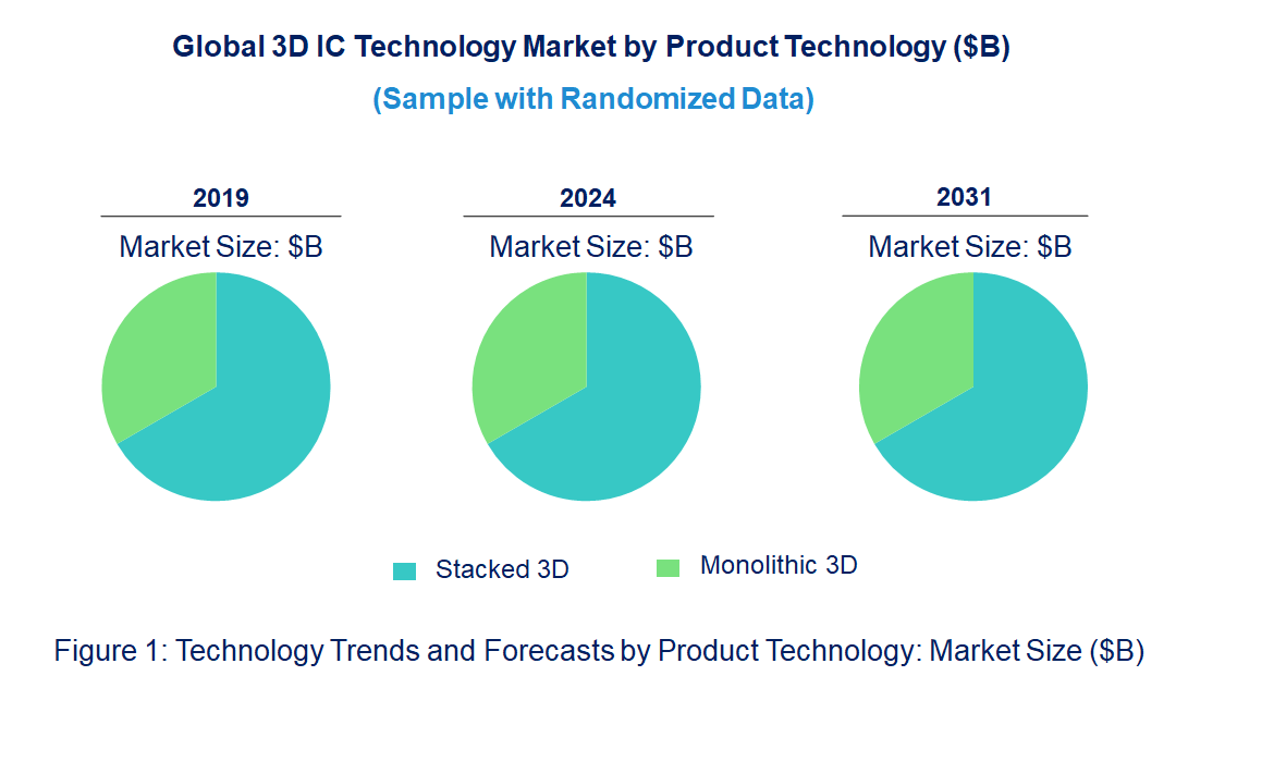
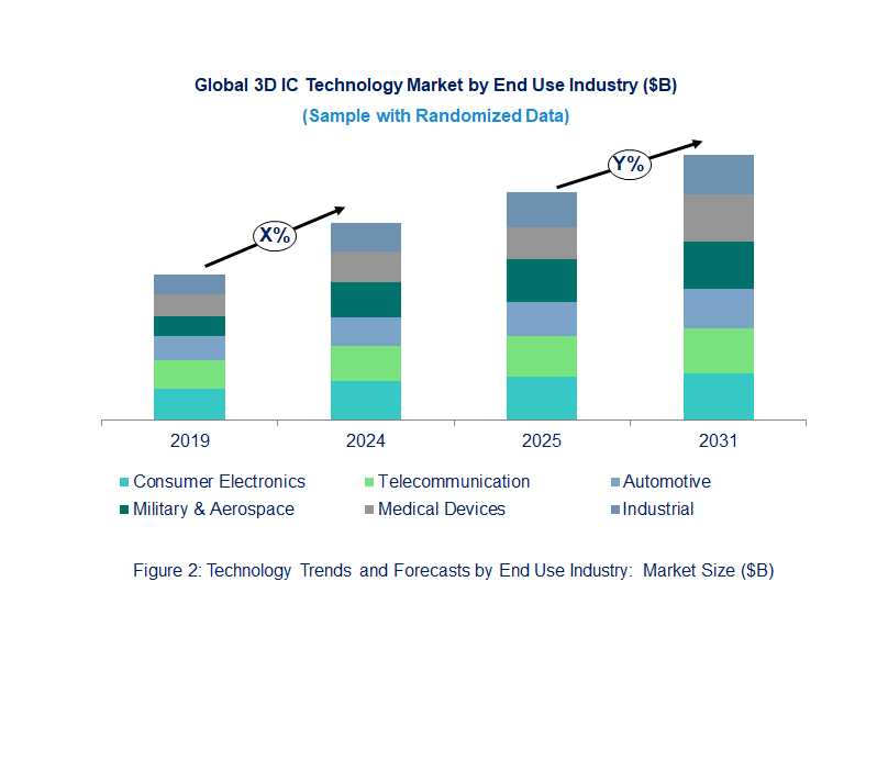
• Hybrid Bonding, which Improves Performance: The use of hybrid bonding techniques is becoming a primary trend in 3D integration, where layers of different materials are used individually. This trend replaces traditional bonding methods, such as copper pillar or TSV bonding, which degrade overall electrical and thermal performance, especially when memory and logic are integrated at high density. The ability to integrate fine-pitch interconnects on the surface of a chip greatly extends its use in cases like 5G technologies and AI applications, where high bandwidth and low latency rendering are desired.
• New Penetrating Technologies Enabling Advanced Packaging Solutions: These technologies enable better integration of complex systems while reducing signal losses and improving thermal performance. Advanced packaging is increasing the density and performance of interconnects and integrating dissimilar materials, making smaller, faster, and more functional chips for mobile, automotive, and AI systems.
• Inclusion of AI and Machine Learning Factors: The inclusion of artificial intelligence (AI) and machine learning (ML) factors in 3D integrated circuit design is increasing, especially for data centers, edge computing, and driverless vehicle applications. AI operations can be performed more intelligently with lower chip-to-chip communication latency by placing memory and processing units in the same three-dimensional space. This trend is critical for real-time operations, such as image or language processing, that demand high-speed computation.
• Miniaturization and Power Dissipation: Miniaturization remains one of the most impactful trends in the 3D IC market. The increased number of circuitry layers needed to form a single device results in a smaller, faster device. This trend is particularly important for consumer electronic devices that need to be compact, lightweight, and portable. Additionally, 3D ICs enable low-power designs, where power consumption is reduced by using fewer interconnects for data transmission, which is important for mobile and IoT devices.
• Increased Adoption in Emerging Markets like Automotive and IoT: The growing demand for intelligent and connected devices is driving the automotive and IoT sectors to adopt 3D IC technology more rapidly. For automotive applications such as advanced driver-assistance systems (ADAS), autonomous vehicles, and electric vehicles, where chip area is always at a premium, 3D ICs are critical. Even in the IoT domain, 3D ICs are being integrated to enable innovations like smart sensors, connected devices, wearables, and other edge devices that require large amounts of data to be processed, due to their small size and low power requirements. These advancements are shaping the growth of the IC market by improving the performance, effectiveness, and functionality of various industries. 3D integration, AI chip integration, package miniaturization, and increased adoption in the automotive and IoT industries are expanding the applications of 3D IC technology, highlighting what semiconductors can achieve. The 3D IC market will be a key driver in the development of new electronic products and systems in combination with these innovations.
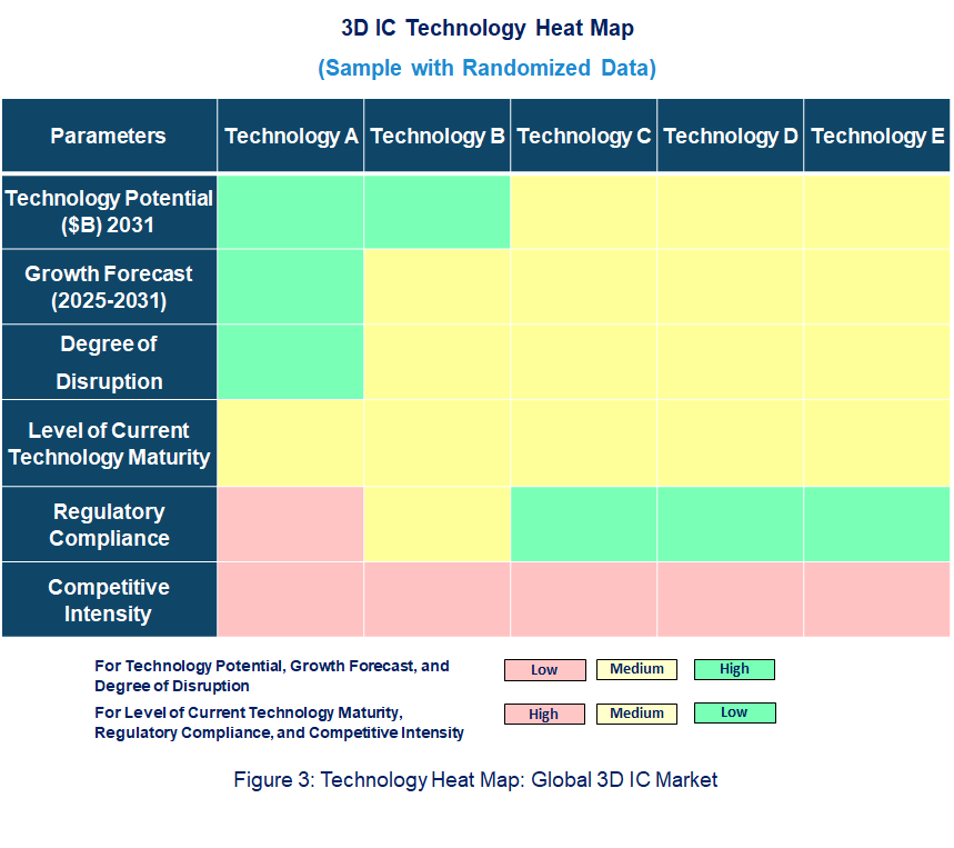
• Potential in Technology: The technology’s potential lies in addressing the limitations of 2D scaling and enabling continued adherence to Moore’s Law, especially for high-performance computing, AI, and data center applications.
• Degree of Disruption: The degree of disruption is high, as 3D ICs challenge traditional packaging methods and redefine chip design, integration, and interconnect strategies. Companies adopting 3D ICs can achieve higher functionality per footprint, revolutionizing products in consumer electronics and enterprise systems.
• Current Technology Maturity Level: However, the current technology maturity varies. While Through-Silicon Via (TSV)-based 3D ICs and memory stacking (e.g., HBM, 3D NAND) are commercially available and well-understood, logic stacking and heterogeneous integration are still evolving.
• Regulatory Compliance: Regulatory compliance is a developing area, particularly in thermal management, reliability testing, and manufacturing standards. As complexity increases, industry stakeholders must align on testing, inspection, and quality assurance frameworks. Overall, 3D IC technology is moving rapidly from innovation to adoption, promising a future of compact, energy-efficient, and high-performance devices while requiring substantial investment in design tools, infrastructure, and compliance systems.
• United Microelectronics (UMC): With the increasing demand for high-performance chips, UMC has focused on increasing its investment in advanced packaging technologies, namely 3D ICs. It is already positioned in the integration of stacked wafers that utilize fine pitch interconnects and TSVs, effectively targeting the AI and automotive chip markets.
• Tezzaron Semiconductor: The power of 3D integrated circuits seems to still be encapsulated by Tezzaron Semiconductor with its proprietary 3D wafer-level stacking technology. Specifically, its focus has been on improving thermal performance, interconnect density, and yield rate for integrated memory and logic circuits in stacked configurations. This technology has huge potential applications in consumer electronics and communications, promising high-volume throughput integrated in single packages.
• 3M: 3M has been engaged in the development of advanced materials for 3D integrated circuits (ICs), including recent developments in thermal interface materials (TIMs) and other areas such as conductive adhesives. Its solutions facilitate thermal management and reliability enhancement of stacked ICs, which is important in protecting devices with high density, high speed, and performance, particularly in the telecom, automotive, and aerospace sectors.
• IBM Corporation: IBM has made strides in the further development of 3D ICs, particularly in memory integration and memory packaging. Its partnership with dominant companies in the field of bonding technologies would enhance the possibility of integrating logic with memory on the same die. This is an important step in improving the performance of cloud-based applications, artificial intelligence, and workloads in data centers.
• Xilinx: Xilinx has been working on the innovative development of heterogeneous integration, enabling 3D ICs composed of various chip types in one package, such as FPGA and memory. Its work on 3D ICs is mainly focused on powerful applications like the 5G network and artificial intelligence workloads, which require low latency and high throughput.
• Monolithic 3D: Monolithic 3D is the new player in 3D ICs as it develops techniques for stacking transistor layers on top of each other, done on a single base instead of multiple layers. By stacking transistors on top of a substrate, this technology helps sidestep the need for TSVs, making 3D ICs less complex and costly. With the endless possibilities this technique presents, the strategy reimagines low-cost, high-performance products, especially aimed at IoT and consumer electronics.
• Intel Corporation: The constant innovation by Intel has allowed the company to not only lead the competition but to become the competition in 3D IC devices through advancements like the Foveros packaging platform. It supports packaging technology that increases the supply of attractive chiplets with robust interconnects, enabling greater flexibility across subsystems and improving efficiency, which other companies lack. The market strategies developed by Intel provide the only technology that industries in AI, mobile, high-performance computing, and others desperately need.
• Toshiba Corp: Toshiba’s 3D IC technologies have enhanced memory composition, specifically with the incorporation of NAND flash memory. These developments in 3D NAND technology have changed the landscape of data storage, allowing for higher memory density in smaller sizes, which is especially needed in modern devices such as phones, tablets, cloud storage, and home appliances.
• Amkor Technology: Amkor Technology is very active in the advanced development and provision of services related to the packaging of 3D integrated circuits. Its expertise in chip stacking and TSV technology has allowed for increased performance and reliability of stacked ICs. Amkor’s solutions are instrumental in the growing demand for high-performance chips, which find applications in assembling telecommunication equipment, automotive, and home appliances.
• Samsung Electronics: Samsung has been a strong player in the 3D IC market for memory and logic integration applications. The incorporation of 3D NAND flash memory into its products has proven to increase storage density and reduce storage costs. Samsung aims to package its memory products with 3D ICs that are suitable for AI, data centers, and consumer devices. Such improvements are aiding the growth of 3D IC technologies’ adoption across diverse industries through improved performance standards, reduced power usage, and smaller, more effective modules. Innovations from these key players will see the role of 3D IC technology become even more pronounced in the future of computing, storage, and networking solutions.
• The Shrinking Size of Electronic Devices: The higher demand for smaller, lighter devices that perform more work has pushed the need for 3D IC adoption. By stacking several layers of chips on top of each other, superior performance can be achieved within a smaller volume using high-density integration. This is especially useful for smartphones and wearables, which are considered consumer electronics.
• AI and High-Performance Computers: Another key factor enabling 3D communication between the layers is the growing need for AI, machine learning, and high-performance computers (HPC). With improved memory integration and faster data processing, 3D ICs offer the fast communication required by most AI-related applications.
• Refinement of Packaging Technologies: As semiconductor devices become more sophisticated, packaging technologies such as 3D ICs are becoming more important. These technologies allow the integration of various types of chips—memory, logic, and sensors—thereby minimizing power consumption and enhancing overall device performance, especially in the IoT and automotive sectors.
• The Automotive and Mass IoT Market: With the rise of autonomous vehicles (AVs) and IoT devices, which are expected to use 3D integrated circuits with high-density, low-power chips, 3D ICs have grown in popularity. It is particularly critical in these sectors to efficiently and precisely integrate sensors, processors, and memory, as the performance efficiencies realized in sensors, due to lower energy consumption, are significant.
• More Efficient Manufacturing Practices: Hybrid bonding and TSV (Through-Silicon Vias) are advancements that may enhance the prospects of establishing 3D ICs. These developments are projected to improve yields, reduce defects, and decrease production costs, thereby speeding up the incorporation of 3D ICs into common applications. Challenges:
• Pricing and Complexity Issues: The complexity of 3D IC manufacturing, including layer stacking, bonding, and interconnects, increases the cost of production. Suitable regimes need to be created so that 3D integrated circuits can be applied to lower-cost consumer products, addressing the most important challenge of high capital investment in equipment and skilled labor.
• Handling Thermal Issues: 3D ICs are impressive in the amount of data they can handle, not to mention the number of layers in which they are designed. On the other hand, stacking the layers together makes heat dissipation a difficult task. Heat dissipation is key to ensuring ideal operability and maintaining the structural integrity of 3D ICs. For wider adoption, more efficient cooling materials and methods are required.
• Integration and Yield Constraints: The integration of materials, and more importantly, layers when creating 3D ICs can cause yield issues. For instance, a defect in a single layer can damage the entire core. The potential for significant defect rates, along with complicated processes for interconnecting stacked layers, may impede the growth and efficiency of 3D ICs.
• Market Acceptance and Critical Mass: The reliability of 3D ICs is still in question. Market acceptance remains a challenge, as the technology needs to overcome the barriers of size, efficiency, and integration complexity before it can achieve critical mass.
• United Microelectronics
• Tezzaron Semiconductor
• 3M
• IBM Corporation
• Xilin
• Monolithic 3D
• Technology Readiness by Technology Type: Stacked 3D IC technology is at a high technology readiness level (TRL), especially for memory applications like HBM and 3D NAND, with extensive deployment across servers, GPUs, and smartphones. It enjoys strong industry adoption, high competition, and robust compliance protocols. Monolithic 3D ICs, in contrast, are at a moderate TRL, with active prototyping in logic stacking and ongoing research in heat-sensitive materials and process alignment. Stacked 3D is used in bandwidth-intensive applications, while Monolithic 3D is positioned for ultra-dense, energy-efficient logic integration in AI and mobile devices. Competitive intensity is currently higher in stacked solutions, while monolithic faces future disruption potential. Regulatory standards are still evolving for monolithic architectures.
• Competitive Intensity and Regulatory Compliance: The Stacked 3D IC market is highly competitive, with major players like Intel, Samsung, and TSMC investing heavily in TSV-based solutions. Regulatory compliance focuses on reliability, thermal management, and standardization of testing. Monolithic 3D ICs face less competitive pressure due to lower commercial maturity, but R&D race is intense among research labs and startups. Monolithic approaches face stricter regulatory hurdles due to heat dissipation, material integrity, and complex fabrication steps. Stacked 3D ICs benefit from existing regulatory frameworks and global supply chain compatibility. Both face scrutiny over long-term reliability, cross-layer interactions, and yield optimization.
• Disruption Potential by Technology Type: Stacked 3D IC technology, utilizing Through-Silicon Vias (TSVs), is already transforming memory and high-performance computing by enabling greater bandwidth and efficiency. It disrupts traditional 2D integration by dramatically reducing form factor and interconnect delay. Monolithic 3D ICs, which build transistors layer by layer on a single wafer, present a deeper level of disruption by enabling true logic-on-logic integration with ultra-short interconnects. While Stacked 3D ICs are more mature and commercially available, Monolithic 3D ICs offer future potential for finer-grain integration at lower power and cost. Monolithic technology, however, is still in early stages, limited by thermal and manufacturing challenges. Both types could redefine device architecture across AI, IoT, and mobile. Their adoption promises smaller, faster, and more power-efficient chips that break conventional scaling limits.
• Stacked 3D
• Monolithic 3D
• Consumer Electronics
• Telecommunication
• Automotive
• Military & Aerospace
• Medical Devices
• Industrial
• North America
• Europe
• Asia Pacific
• The Rest of the World
• Latest Developments and Innovations in the 3D IC Technologies
• Companies / Ecosystems
• Strategic Opportunities by Technology Type


Choose a license that fits your team. Instant PDF delivery.
Prices exclude taxes. Instant delivery. Custom licensing available on request.
Market Report · May 18, 2026
Market Report · May 18, 2026
Market Report · May 18, 2026
Trusted partner for strategic intelligence and business growth


Receive a complimentary market analysis tailored to your industry. Our analysts will identify key growth opportunities and competitive dynamics specific to your business.

Market size, growth rate, and key trend analysis for your specific sector.

Top competitor positioning and market share analysis.

Strategic recommendations backed by data-driven insights.
Get curated market intelligence and competitive moves straight to your inbox.
By subscribing, you agree to receive our monthly insights. Unsubscribe anytime.
Receive a complimentary market analysis tailored to your industry. Our analysts will identify key growth opportunities and competitive dynamics specific to your business.
Market size, growth rate, and key trend analysis for your specific sector.
Top competitor positioning and market share analysis.
Strategic recommendations backed by data-driven insights.
Get curated market intelligence, emerging trends, and competitive moves straight to your inbox each month.
By subscribing, you agree to receive our monthly insights. Unsubscribe anytime.
We'll send your sample report shortly.