
Market Report · May 18, 2026

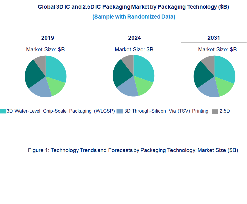
This market report covers trends, opportunities, and forecasts in the global 3d ic and 2.5d ic packaging market to 2031 by packaging technology (3d wafer-level chip-scale packaging (wlcsp), 3d through-silicon via (tsv), and 2.5d), end use industry (consumer electronics, industrial, telecommunications, automotive, military & aerospace, medical devices, and others), and region (North America, Europe, Asia Pacific, and the Rest of the World)
We'll send your sample report shortly.
![3D IC and 2.5D IC Packaging Market Trend and Forecast by End Use Industry [Value from 2019 to 2031]:](https://lucintel.com/images/3D-IC-and-2.5D-IC-Packaging-Market-Segment.png "3D IC and 2.5D IC Packaging Market Trend and Forecast by End Use Industry [Value from 2019 to 2031]:")
• Heterogeneous Integration: Heterogeneous integration is picking up because it allows for the integration of different types of chips, such as logic, memory, and RF, into one package. This method optimizes system performance and functionality while reducing size and cost. Heterogeneous integration allows for more design flexibility and enables innovation areas such as AI applications, autonomous systems, and 5G applications. Advanced Interposer Technologies: Advancements in interposers, especially in silicon and organic materials, are taking the 2.5D IC packaging to new heights. These interposers lead to higher interconnect density, better thermal management, and low power consumption. Impact: Improved interposer technologies result in faster data transfer and reliability, which is essential for high-performance computing and data centers.
• Through-Silicon Via (TSV) Optimization: TSVs are crucial in 3D IC packaging so that chips can be stacked vertically with proper communication pathways. The optimization of TSVs can be done by reducing their size, improving yield, and minimizing costs. Impact: TSV advancements improve scalability and make new application possibilities for smaller, faster, and power-efficient device designs open.
• Chiplet-based architectures: The chiplet approach enables manufacturers to integrate smaller blocks of tested functions into a larger package. This method reduces development time, cost, and complexity while improving performance and scalability. Impact: Chiplet-based architectures enable customization and speed innovation in consumer electronics, automotive systems, and AI workloads.
• Improving thermal management solutions: In light of growing power densities, advanced thermal management solutions are necessary. Technologies like microfluidic cooling, advanced thermal interface materials, and integrated heat spreaders should be developed to overcome thermal challenges. Impact: Efficient thermal management ensures high reliability and extended lifespan of operation for high-performance devices, thus ensuring sustained efficiency. Emerging trends in 3D IC and 2.5D IC packaging technologies are fundamentally reshaping the semiconductor landscape. Heterogeneous integration, optimized TSVs, advanced interposers, and other innovations are addressing critical performance, scalability, and efficiency challenges. These emerging trends are not only driving the development of smaller and more powerful devices but also accelerating AI, 5G, and other high-growth sectors, laying the groundwork for what will be the next generation of technological advancements.
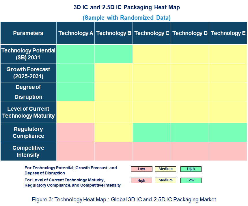
• Potential in Technology: The 3D IC and 2.5D IC packaging market holds immense potential, revolutionizing the semiconductor industry by enabling greater integration, performance, and miniaturization of electronic devices. These advanced packaging technologies allow for stacking or horizontally integrating multiple semiconductor chips, improving speed, power efficiency, and memory bandwidth while reducing overall size. The potential applications span from high-performance computing (HPC), artificial intelligence (AI), and data centers to consumer electronics, making them essential for next-generation technologies.
• Degree of Disruption: The degree of disruption is significant, as 3D IC and 2.5D IC packaging are reshaping traditional semiconductor designs. These technologies enable better chip interconnectivity and reduced signal loss, which is crucial for applications requiring high data throughput and low latency. This disruption impacts a wide range of industries, from cloud computing to mobile devices, offering enhanced performance and new capabilities that were not possible with traditional packaging methods.
• Current Technology Maturity Level: The maturity level of 3D IC and 2.5D IC packaging technologies is advancing but still faces challenges. While some commercial applications are available, especially in memory and high-performance processors, the scalability, cost, and thermal management issues remain obstacles to widespread adoption. As the technology evolves, solutions to these challenges are improving.
• Regulatory Compliance: Regulatory compliance in the 3D IC and 2.5D IC packaging market is still developing. Given the complexity of these advanced packaging methods, manufacturers must comply with environmental and safety standards, particularly in handling hazardous materials during fabrication. As the market expands, regulatory bodies will likely refine their standards for this emerging technology.
• Taiwan Semiconductor Manufacturing (TSMC) TSMC has developed its sophisticated CoWoS (Chip-on-Wafer-on-Substrate) and SoIC (System on Integrated Chips) technologies to support higher bandwidth and higher integration densities.
• Samsung Electronics Samsung further developed its X-Cube 3D package technology with TSV integration for faster data transfer and excellent thermal performance.
• Toshiba Toshiba is putting much emphasis on 2.5D packaging for its high-performance memory modules by using interposer technologies to enhance reliability and scalability.
• Advanced Semiconductor Engineering (ASE): ASE is expanding its fan-out wafer-level packaging capabilities with hybrid bonding techniques to enhance design flexibility.
• Amkor Technology: Amkor is investing in silicon interposer and wafer-level integration technologies focusing on yield improvement and cost reduction.
• Growing Demand for High-Performance Computing As more AI, IoT, and 5G applications continue to grow, 3D and 2.5D ICs are sought for their advancements in faster processing of data and lower latency. Miniaturization of Devices Efficiency in space consumption has transformed consumers’ demand for compact, multifunctional electronics, creating a drive for manufacturers to take up these technologies.
• Energy Efficiency Constraints The growing importance of sustainability calls for energy-efficient packaging solutions and, ultimately, for high-performance advanced IC designs to be developed. Impact: Saves power consumption in both data centers and portable devices and aligns with environmental goals.
• Growth in Heterogeneous Integration The ability to integrate different chip types in a single package enables manufacturers to optimize the performance and function of the packaging. Impact: Improves flexibility and scalability for prospects in the advancement of autonomous systems and AI-based applications.
• Advancements in Manufacturing Technologies Innovations in TSVs, interposers, and thermal management techniques are decreasing the cost and increasing the yield. Impact: Promotes market growth since it makes 3D IC and 2.5D IC packaging more available to manufacturers. Key Challenges
• High Manufacturing Cost The complex processing and materials used in this technology drive up production costs.
• Thermal Management Issues The problem of heat dissipation in 3D ICs with dense packing threatens the reliability and performance of the structure.
• Intricate Design and Testing Processes Ensuring functionality as well as compatibility in 3D and 2.5D IC designs necessitates sophisticated design tools and methodologies.
• Yield and Scalability Issues Low yields in the manufacturing process are a result of TSVs and interposers’ defects, which do not support high-volume production.
• Regulatory and Material Constraints Environmental and safety requirements can be a limiting factor in the choice of materials and technologies. Technology advancement and the requirement for high-performance and compact devices are driving 3D IC and 2.5D IC packaging. However, technological challenges, high cost, high temperature issues, and regulatory constraints will impact growth. Together, these factors set the course for the market, which continues to be innovative and transformative for the semiconductor industry.
• Taiwan Semiconductor Manufacturing
• Samsung Electronics
• Toshiba
• Advanced Semiconductor Engineering
• Amkor Technology
• Technology Readiness by Technology Type: Readiness and market influence vary for 3D Wafer-Level Chip-Scale Packaging (WLCSP), 3D Through-Silicon Via (TSV), and 2.5D Packaging technologies. WLCSP technology has a very high level of readiness; it is extensively utilized for compact mobile devices. 3D TSV presents itself as being advanced but suffers from yield and thermal management issues to be applied in high-performance computing and AI applications. 2.5D packaging, by using interposers, bridges the gap between scalable integration for IoT and automotive sectors. Each of the technologies is needed to address competitive pressures and meet regulations regarding safety, environmental impact, and waste management to unlock its full potential.
• Competitive Intensity and Regulatory Compliance: Rivalry is intensifying across technologies such as Atomic Clocks, Magnetic Sensors, PAR 3D IC and 2.5D IC Packaging, and Gravity Sensors, since differentiation by innovation and performance characterizes their moves. Atomic Clocks and Gravity Sensors value precision and reliability, where the applications lie in aerospace and scientific research, while Magnetic Sensors are directed to automobile and IoT demands. High-density integration for semiconductors is the goal of PAR 3D IC technologies, raising the ante in competition among manufacturers. Regulatory compliance is highly important, with key requirements in using correct materials, safety measures, and environmental compliance. This ensures marketplace sustainability and global competitiveness.
• Disruption Potential of Various Technologies in 3D IC and 2.5D IC Packaging: Some of the dominant technologies within 3D IC and 2.5D IC packaging involve Through-Beam, Retro-Reflective, and Reflective. These types of systems ensure high accuracy and reliability in quality control, thereby ensuring proper alignment in chip stacking processes. In the manufacturing process, Retro-Reflective methods increase automation as they provide feedback to the sensor in compact spaces, which is a requirement for efficient lines of assembly. Reflective technologies can detect irregularities on surfaces, thus producing defect-free interposers and TSVs. These technologies help drive innovation, reduce error rates, and increase yield rates in advanced IC packaging solutions for scalability and cost-effectiveness.
• 3D Wafer-Level Chip-Scale Packaging (WLCSP)
• 3D Through-Silicon Via (TSV)
• 2.5D
• Consumer Electronics
• Industrial
• Telecommunications
• Automotive
• Military & Aerospace
• Medical Devices
• Others
• North America
• Europe
• Asia Pacific
• The Rest of the World
• Latest Developments and Innovations in the 3D IC and 2.5D IC Packaging Technologies
• Companies / Ecosystems
• Strategic Opportunities by Technology Type


Choose a license that fits your team. Instant PDF delivery.
Prices exclude taxes. Instant delivery. Custom licensing available on request.
Market Report · May 18, 2026
Market Report · May 18, 2026
Market Report · May 18, 2026
Trusted partner for strategic intelligence and business growth


Receive a complimentary market analysis tailored to your industry. Our analysts will identify key growth opportunities and competitive dynamics specific to your business.

Market size, growth rate, and key trend analysis for your specific sector.

Top competitor positioning and market share analysis.

Strategic recommendations backed by data-driven insights.
Get curated market intelligence and competitive moves straight to your inbox.
By subscribing, you agree to receive our monthly insights. Unsubscribe anytime.
Receive a complimentary market analysis tailored to your industry. Our analysts will identify key growth opportunities and competitive dynamics specific to your business.
Market size, growth rate, and key trend analysis for your specific sector.
Top competitor positioning and market share analysis.
Strategic recommendations backed by data-driven insights.
Get curated market intelligence, emerging trends, and competitive moves straight to your inbox each month.
By subscribing, you agree to receive our monthly insights. Unsubscribe anytime.
We'll send your sample report shortly.